Unit 3: 8051 Architecture
Comprehensive guide to 8051 microcontroller architecture and components
General Block Diagram of a Microcontroller
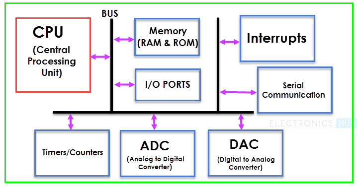
Understanding the Core Components and Their Interconnections
-
CPU (Central Processing Unit)
- ALU (Arithmetic Logic Unit): The heart of calculations and logic operations. Performs arithmetic (addition, subtraction, etc.), logical (AND, OR, NOT) comparisons, and data manipulation.
- Control Unit (CU): The manager that fetches instructions from memory, decodes them, and generates control signals to orchestrate the actions of all components within the microcontroller.
- Registers: Small, incredibly fast memory units built into the CPU for temporarily storing data, instructions, and intermediate results.
-
Memory
- ROM (Read-Only Memory): Non-volatile memory used to permanently store the microcontroller's firmware (program code) and essential data.
- RAM (Random Access Memory): Volatile memory for storing temporary data and variables used while the microcontroller is running a program.
- Flash Memory: In modern microcontrollers, flash memory often replaces traditional ROM for its flexibility, offering reprogrammable program memory.
-
I/O Ports (Input/Output Ports): Versatile pins that can be configured as either inputs or outputs.
- Inputs: Connect to external sensors, switches, keypads, and other input devices that provide information to the microcontroller.
- Outputs: Drive LEDs, displays, motors, actuators and other devices for interacting with the external world.
-
Bus System: A communication network of wires connecting the CPU, memory, I/O ports, and other components.
- Address Bus: Carries memory addresses to specify locations for data transfer.
- Data Bus: Transfers data between the various components.
- Control Bus: Transmits control signals (read/write, timing, etc.) to synchronize operations.
-
Timers/Counters: Specialized modules for:
- Generating Accurate Time Delays: Essential for controlling the timing of operations.
- Counting External Events: Measuring frequencies, pulse widths, and more.
- Output Waveform Generation: Like Pulse Width Modulation (PWM) for motor control, dimming LEDs, etc.
-
Serial Port: Facilitates communication with other devices using standard protocols like:
- UART: Universal Asynchronous Receiver/Transmitter (common for simple serial communication).
- SPI, I2C: For interfacing with various sensors and peripherals.
-
Interrupts: Signals that allow the microcontroller to respond to high-priority events immediately
- External Interrupts: Triggered by changes on input pins (e.g., button presses).
- Internal Interrupts: Generated by timers, ADCs, or other peripherals.
-
ADC (Analog to Digital Converter): Converts incoming analog signals (e.g., from temperature sensors) into digital values that the CPU can process.
-
DAC (Digital to Analog Converter): Transforms digital data from the CPU into analog signals useful for driving devices like speakers or creating smooth control voltages.
-
On-Chip Oscillator: Provides the internal clock signal that drives the microcontroller's timing.
-
Special Function Registers (SFRs): Registers dedicated to controlling the configuration and operation of the microcontroller's peripherals.
Pin Diagram of 8051
The following image shows the 8051 Microcontroller Pin Diagram with respect to a 40 – pin Dual In-line Package (DIP).
Pins 1 – 8 (PORT 1):
-
Pins 1 to 8 are the PORT 1 Pins of 8051. PORT 1 Pins consists of 8 – bit bidirectional Input / Output Port with internal pull – up resistors. In older 8051 Microcontrollers, PORT 1 doesn’t serve any additional purpose but just 8 – bit I/O PORT.
-
In some of the newer 8051 Microcontrollers, few PORT 1 Pins have dual functions. P1.0 and P1.1 act as Timer 2 and Timer 2 Trigger Input respectively.
-
P1.5, P1.6 and P1.7 act as In-System Programming Pins i.e. MOSI, MISO and SCK respectively.
Pin 9 (RST): Pin 9 is the Reset Input Pin. It is an active HIGH Pin i.e. if the RST Pin is HIGH for a minimum of two machine cycles, the microcontroller will be reset. During this time, the oscillator must be running.
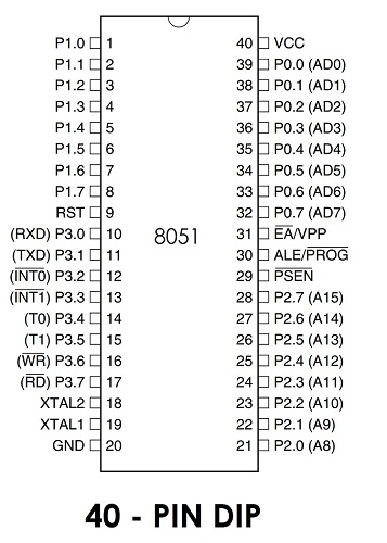
Pins 10 – 17 (PORT 3): Pins 10 to 17 form the PORT 3 pins of the 8051 Microcontroller. PORT 3 also acts as a bidirectional Input / Output PORT with internal pull-ups. Additionally, all the PORT 3 Pins have special functions. The following table gives the details of the additional functions of PORT 3 Pins.
| PORT 3 Pin | Function | Description |
|---|---|---|
| P3.0 | RXD | Serial Input |
| P3.1 | TXD | Serial Output |
| P3.2 | INT0 | External Interrupt 0 |
| P3.3 | INT1 | External Interrupt 1 |
| P3.4 | T0 | Timer 0 |
| P3.5 | T1 | Timer 1 |
| P3.6 | WR | External Memory Write |
| P3.7 | RD | External Memory Read |
Table: PORT 3 Pins
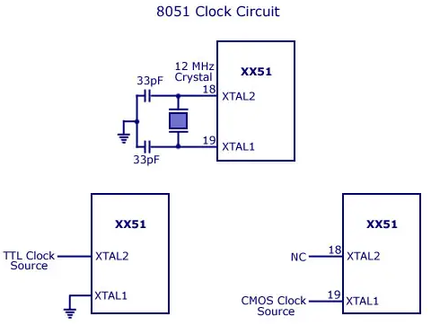
Pins 18 & 19: Pins 18 and 19 i.e. XTAL 2 and XTAL 1 are the pins for connecting external oscillator. Generally, a Quartz Crystal Oscillator is connected here.
Pin 20 (GND): Pin 20 is the Ground Pin of the 8051 Microcontroller. It represents 0V and is connected to the negative terminal (0V) of the Power Supply.
Pins 21 – 28 (PORT 2): These are the PORT 2 Pins of the 8051 Microcontroller. PORT 2 is also a Bidirectional Port i.e. all the PORT 2 pins act as Input or Output. Additionally, when external memory is interfaced, PORT 2 pins act as the higher order address byte. PORT 2 Pins have internal pull-ups.
Pin 29 (PSEN): Pin 29 is the Program Store Enable Pin (PSEN). Using this pins, external Program Memory can be read.
Pin 30 (ALE/PROG): Pin 30 is the Address Latch Enable Pin. Using this Pins, external address can be separated from data (as they are multiplexed by 8051). During Flash Programming, this pin acts as program pulse input (PROG).
Pin 31 (EA/VPP): Pin 31 is the External Access Enable Pin i.e. allows external Program Memory. Code from external program memory can be fetched only if this pin is LOW. For normal operations, this pins is pulled HIGH. During Flash Programming, this Pin receives 12V Programming Enable Voltage (VPP).
Pins 32 – 39 (PORT 0): Pins 32 to 39 are PORT 0 Pins. They are also bidirectional Input / Output Pins but without any internal pull-ups. Hence, we need external pull-ups in order to use PORT 0 pins as I/O PORT. In addition to acting as I/O PORT, PORT 0 also acts as lower order address/data bus when external memory is accessed.
Pin 40 (VCC): Pin 40 is the power supply pin to which the supply voltage is given (+5V).
8051 Microcontroller Block Diagram
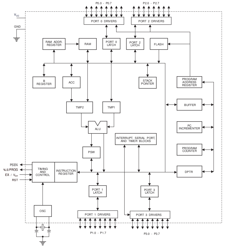
Central Processing Unit (CPU)
- ALU (Arithmetic Logic Unit): The heart of calculations and logic operations. Performs arithmetic (addition, subtraction, etc.), logical (AND, OR, NOT) comparisons, and data manipulation.
- Instruction Decoder: Decodes the instruction and generates control signals for other parts of the CPU.
- Timing and Control Unit: Manages the fetch-decode-execute cycle of the CPU and synchronizes actions with other blocks.
Registers
- Accumulator (A): An 8-bit register used for most arithmetic and logical operations.
- B Register: An 8-bit temporary register used for multiplication, division, and other data manipulation.
- Program Status Word (PSW): Holds status flags like carry, overflow, parity, and register bank selection.
- Stack Pointer (SP): Points to the top of the stack in RAM, used for subroutine calls and data storage.
- Program Counter (PC): Keeps track of the memory address of the next instruction to be fetched.
- DPTR: This is 16 bit register made up of two 8 bit registers – DPH & DPL. This register is used to point to Internal or External memory location.
- SFR: Special Function Registers (SFRs) are special registers that contains control and status bits for Timer/Counter (TCON, TMOD), Interrupts (IE, IP), Serial Communication (SCON) and Power Control (PCON).
- Instruction Register: Holds the currently fetched instruction.
Memory
- Internal RAM (128 bytes): Stores temporary data and variables during program execution.
- Register Banks 0-3: Four sets of eight 8-bit general-purpose registers.
- Bit-addressable area (20h-2Fh): 16 bytes with individually addressable bits.
- General-purpose area (30h-7Fh): Remaining 80 bytes for data and variables.
- Internal ROM (typically 4KB): Stores the program code of the microcontroller.
Input/Output (I/O)
- Ports 0-3 (P0-P3): Four 8-bit I/O ports that can be individually configured as input or output pins.
Timers/Counters
- Timers/Counters 0 and 1 (T0, T1): 16-bit timers/counters that can be used for various purposes like measuring time intervals, counting external events, and generating waveforms.
Serial Port (UART)
- TXD (Transmit Data): Transmits serial data out of the microcontroller.
- RXD (Receive Data): Receives serial data into the microcontroller.
- SBUF (Serial Buffer): Temporarily stores data during serial transmission or reception.
Interrupts
- External Interrupts (INT0, INT1): Triggered by signals on external pins.
- Timer Interrupts (TF0, TF1): Triggered when timers overflow or reach a specific value.
- Serial Interrupts (RI, TI): Triggered by events related to serial communication.
- Interrupt Control Logic: Manages the enabling/disabling, prioritizing, and handling of interrupts.
Additional Notes
- Bus Structure: The 8051 uses an internal data bus to connect the CPU, memory, and I/O blocks. Instructions and data flow along this bus under the control of the CPU.
- Reset: The RESET input initializes the 8051, setting registers and the Program Counter to their starting states.
- Oscillator: The XTAL1 and XTAL2 inputs connect to the crystal and other components that generate the clock signal for the microcontroller.
ALU (Arithmetic Logic Unit) & Timing and Control Unit
8051 ALU (Arithmetic Logic Unit)
-
The Computational Heart: The ALU is responsible for executing the core calculations and logical manipulations within the 8051 microcontroller. As its name suggests, it handles two primary types of operations:
-
Arithmetic Operations
- Addition (
ADD) - Subtraction (
SUBB) - Multiplication (
MUL) - Division (
DIV) - Incrementing (
INC) - Decrementing (
DEC)
- Addition (
-
Logical Operations
- AND (
ANL) - OR (
ORL) - Exclusive-OR (
XRL) - NOT (
CLR,CPL) - Comparisons (for setting flags in the PSW register)
- AND (
-
Key Components:
- Accumulator: Data typically flows in and out of the Accumulator (A Register) during ALU operations.
- Temporary Register: Holds the second operand during calculations.
- Arithmetic/Logic Circuits: The actual hardware circuitry that performs the computations and manipulations.
-
Relationship to PSW: The ALU interacts closely with the PSW register. ALU operations set flags like Carry (CY), Auxiliary Carry (AC), Overflow (OV), and Parity (P) in the PSW, which then become decision points for control flow in the program.
8051 Timing and Control Unit
-
Conductor of the Orchestra: The Timing and Control Unit is the mastermind that synchronizes all the actions within the 8051 microcontroller. It ensures everything happens at the right time and in the correct sequence.
-
Key Functions:
- Instruction Fetching and Decoding: Fetches instructions from memory and interprets their meaning, figuring out what actions need to be performed.
- Machine Cycle and State Control: Divides instructions into smaller steps (machine cycles) and generates timing signals that tell each part of the microcontroller when to do what.
- Signal Generation: Produces the precise electrical pulses that activate registers, the ALU, data buses, and other components within the microcontroller.
- Interrupt Handling: Coordinates what happens when an external event (like a timer overflow or a button press) interrupts the currently executing program.
-
Crystal Oscillator's Role: The Timing and Control Unit relies on a crystal oscillator, generating a steady clock signal. This clock signal determines the fundamental speed at which the microcontroller operates.
Instruction Register and Instruction Decoder
Instruction Register (IR)
-
Temporary Holding Area: The Instruction Register is a special, temporary holding space within the microcontroller where the currently fetched instruction resides. It's closely connected to the Instruction Decoder.
-
Size: The size of the Instruction Register typically matches the width of instructions for the microcontroller. In the case of the 8051, instructions can be 1, 2, or 3 bytes long, so the Instruction Register has to accommodate that.
-
Two Main Parts (often): In some architectures, the Instruction Register is divided into:
- Shift Register: Shifts in the instruction, bit by bit, as it's retrieved from memory. This process is synchronized with the microcontroller's clock.
- Hold Register: Holds the fully fetched instruction once the shifting is complete, making it available to the Instruction Decoder.
Instruction Decoder
-
The Translator: The Instruction Decoder is the circuit that analyzes the instruction currently residing in the Instruction Register. It breaks the instruction down into its meaningful components:
-
Opcode: The opcode (operation code) is the part of the instruction that tells the microcontroller what fundamental operation to perform (ADD, MOV, JUMP, etc.).
-
Operands: Operands are the pieces of data the instruction acts upon. This could be register names, immediate data (values hard-coded into the instruction), or memory addresses.
-
Decoding Process: The Instruction Decoder possesses 'knowledge' of all valid instructions in the microcontroller's instruction set. It compares the opcode to this knowledge base to determine:
- What the operation is
- What type of operands are involved
- How many machine cycles are likely needed for execution
-
Control Signal Generation: The Instruction Decoder produces control signals that activate different parts of the microcontroller, ensuring the correct actions are taken for the specified instruction. These signals will direct things like:
- Data transfers from registers to the ALU
- ALU operation selection (add, subtract, etc.)
- Setting of flags in the PSW register
- Flow of data to and from memory
The Dance of Fetching, Decoding, and Execution
-
Fetch: An instruction is retrieved from program memory, often with the help of the Program Counter.
-
Load: The instruction is shifted into the Instruction Register.
-
Decode: The Instruction Decoder analyzes the instruction and generates the appropriate control signals.
-
Execute: The microcontroller, directed by the control signals, carries out the steps required by the instruction.
Accumulator (A)
-
The Workhorse: The Accumulator is the central hub for most arithmetic, logical, and data transfer operations within the microcontroller. If you think of the microcontroller as a tiny calculator, the Accumulator is where you see the numbers being entered and the results being displayed.
-
Key Operations:
- Arithmetic: Addition, subtraction, incrementing, decrementing.
- Logical: AND, OR, XOR, NOT (complements), bit rotations, shifts.
- Data Movement: Transfers data to and from internal RAM or external memory.
-
Special Role in Instructions: Many instructions in the microcontroller's instruction set implicitly use the Accumulator as either the source of data, the destination for the result, or both.
Register B
-
Versatile Assistant: The B Register serves as a secondary register, often used to temporarily hold values to assist in calculations or data manipulation.
-
Specialized Tasks:
- Multiplication and Division: The B Register is essential for the
MUL AB(multiply) andDIV AB(divide) instructions. It holds one of the operands and, in the case of division, stores the remainder of the operation. - Data Manipulation: It can be used as a temporary holding space for values during complex operations that might involve multiple steps.
- Multiplication and Division: The B Register is essential for the
Key Points
- Size: Both the Accumulator and B Register are usually 8-bit registers. This means they can each store a single byte of data (a value from 0 to 255).
- Not General Purpose: Unlike general-purpose registers (like R0, R1, etc. in the 8051), the Accumulator and B Register have more defined roles due to their connection to specific instructions.
PC (Program Counter)
-
The Program's Navigator: The Program Counter holds the address of the next instruction to be executed by the microcontroller. It's like the microcontroller's bookmark within the program.
-
How it Works:
- Fetch: The PC sends its current address to fetch the next instruction from program memory.
- Increment: By default, the PC is automatically incremented after fetching, preparing it for the following instruction.
- Control Flow Changes: Instructions like jumps (
JMP) and calls (CALL) can change the PC's value, altering the program's execution order.
-
Size: The PC is 16 bits wide in the 8051, allowing it to address up to 64KB of program memory.
SP (Stack Pointer)
-
LIFO Storage: The Stack Pointer points to the current 'top' of the stack. The stack is a last-in, first-out (LIFO) data structure within the 8051's internal RAM.
-
Key Operations:
- PUSH: Adds data to the top of the stack. The SP is then decremented to point to the new top.
- POP: Removes data from the top of the stack. The SP is incremented as data is removed.
-
Essential for:
- Subroutines (CALL and RET): Stores the return address when a subroutine is called so the program knows where to resume after the subroutine finishes.
- Interrupt Handling: Stores register values when an interrupt occurs, preserving the state before the interrupt routine is executed.
-
Size: The SP is 8 bits wide in the 8051.
DPTR (Data Pointer)
-
Accessing External Data: The DPTR is a special 16-bit register used for addressing external memory (data memory outside the 8051's internal space).
-
Key Functions:
- Indirect Addressing: The value in DPTR acts as a pointer. Instructions like
MOVX(move external data) use DPTR to specify the source or destination address in external memory. - Lookup Tables: DPTR is useful for storing the starting address of tables or data structures located in external memory.
- Indirect Addressing: The value in DPTR acts as a pointer. Instructions like
Special Function Registers (SFRs)
What is an SFR?
- Special Function Registers (SFRs) are unique memory locations within the 8051 microcontroller's architecture. Unlike general-purpose RAM, SFRs directly control and configure various hardware peripherals and functions of the microcontroller.
- Location: They occupy the address space from 80H to FFH within the internal RAM.
Important 8051 SFRs
| Address (hex) | Register Name | Description |
|---|---|---|
| 80 | P0 | Port 0 (Input/Output) |
| 90 | P1 | Port 1 (Input/Output) |
| A0 | P2 | Port 2 (Input/Output) |
| B0 | P3 | Port 3 (Input/Output) |
| 81 | SP | Stack Pointer |
| 82 | DPL | Data Pointer Low Byte |
| 83 | DPH | Data Pointer High Byte |
| 87 | PCON | Power Control Register |
| 88 | TCON | Timer/Counter 0 Control Register |
| 89 | TMOD | Timer/Counter 0/1 Mode Register |
| 8A | TL0 | Timer/Counter 0 Low Byte |
| 8B | TL1 | Timer/Counter 1 Low Byte |
| 8C | TH0 | Timer/Counter 0 High Byte |
| 8D | TH1 | Timer/Counter 1 High Byte |
| 98 | SCON | Serial Control Register |
| 99 | SBUF | Serial Data Buffer |
| A8 | IE | Interrupt Enable Register |
| B8 | IP | Interrupt Priority Register |
| D0 | PSW | Program Status Word (contains flags) |
| E0 | ACC | Accumulator |
| F0 | B | B Register (auxiliary) |
Table: 8051 SFRs
Here's a breakdown of the most common 8051 SFRs, along with their roles:
1. Accumulator (A)
- Address: E0H
- Function: The heart of most arithmetic and logical operations in the 8051. It acts as a source or destination for data.
2. Program Status Word (PSW)
- Address: D0H
- Function: Contains critical flags indicating the status of the microcontroller, including:
- CY (Carry Flag)
- AC (Auxiliary Carry Flag)
- F0 (User-definable flag)
- RS1, RS0 (Register Bank select bits)
- OV (Overflow Flag)
- P (Parity Flag)
3. B Register (B)
- Address: F0H
- Function: Often used in conjunction with the Accumulator:
- Multiplication and division operations
- Temporary storage of data
4. Timer Registers
- TH0, TL0 (Timer 0): 98H, 99H
- TH1, TL1 (Timer 1): 8AH, 8BH
- Function: Generate time delays, count external events, and form the basis of baud rate generation for serial communication.
5. Serial Port Registers
- SBUF: 99H
- Holds the data to be transmitted (write) or received data (read) during serial communication.
- SCON: 98H
- Controls the mode of serial communication (framing, baud rate, etc.).
6. Interrupt Registers
- IE (Interrupt Enable): A0H
- Enables or disables specific interrupts.
- IP (Interrupt Priority): B0H
- Determines the priority level of different interrupt sources.
7. Port Registers (P0, P1, P2, P3)
- P0: 80H
- P1: 90H
- P2: A0H
- P3: B0H
- Function: Control input and output operations on the 8051's I/O pins.
8. Power Control Register (PCON)
- Address: 87H
- Function: Manages power-saving modes of the 8051 (idle mode, power-down mode).
Note: The exact set of SFRs can vary slightly depending on the specific 8051 microcontroller variant you are using.
How SFRs Work
You can interact with SFRs in your programs just like regular memory locations, using assembly language instructions or C extensions (like sfr, sfr16, and sbit). By manipulating the values in SFRs, you effectively configure the operation of the 8051.
PSW: Program Status Word (Address: 0D0H, Bit addressable)
| PSW.7 | PSW.6 | PSW.5 | PSW.4 | PSW.3 | PSW.2 | PSW.1 | PSW.0 |
|---|---|---|---|---|---|---|---|
| CY | AC | F0 | RS1 | RS0 | OV | - | P |
Table: PSW Register
The PSW register is a vital SFR (Special Function Register) in the functioning of a microcontroller. It reflects the status of the operation that is being carried out in the processor. The PSW register is bit and byte addressable. The physical address of PSW starts from D0H. The individual bits are then accessed using D1, D2 … D7.
| Bit | Description |
|---|---|
| CY | Carry - Is set if data is coming out of bit 7 of Acc during an Arithmetic operation. |
| AC | Auxiliary carry - This bit is set if data is coming out from bit 3 to bit 4 of Acc during an Arithmetic operation. |
| F0 | Flag 0 - User defined flag |
| RS1, RS0 | Register Bank select bits |
| OV | Overflow - OV flag is set if there is a carry from bit 6 but not from bit 7 of an Arithmetic operation. It’s also set if there is a carry from bit 7 (but not from bit 6) of Acc. |
| P | Parity - This bit will be set if ACC has odd number of 1's after an operation. If not, bit will remain cleared. |
Table: PSW Register Bit Function
Register Bank Selection:
| RS1 (PSW.4) | RS0(PSW.3) | Register Bank Selected |
|---|---|---|
| 0 | 0 | RB0 |
| 0 | 1 | RB1 |
| 1 | 0 | RB2 |
| 1 | 1 | RB3 |
Table: Register Bank Selection
Clock & Reset Circuit
Clock Circuit
-
Crystal Oscillator: The foundation of the timing for the 8051 is a crystal oscillator connected to the XTAL1 and XTAL2 pins of the microcontroller.
- The crystal, along with small capacitors (usually in the 20-30pF range), provides a stable and precise clock frequency.
- Common crystal frequencies for 8051 systems are 11.0592 MHz or 12 MHz.
-
Internal Clock Generation: The 8051 has an internal clock generator that takes the external crystal oscillator's signal and divides it down. This ensures that the microcontroller and its various components operate at the correct internal clock speed.
Diagram
Reset Circuit
-
RC Network: A simple resistor-capacitor (RC) network is often used for the reset circuit.
- When power is first applied, the capacitor begins to charge. This holds the RESET pin low for a short period, guaranteeing the 8051 starts in a known state.
- Once the capacitor voltage reaches a threshold, the RESET pin goes high, allowing the microcontroller to begin executing code.
-
Supervisory Circuit (Optional): For more robust reset control, a dedicated supervisory circuit/IC provides more precise monitoring of the power supply voltage. This ensures reliable resets if the power supply fluctuates or becomes unstable.
Diagram
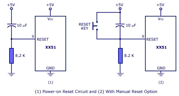
Explanation
- Power On: When the system powers on, the capacitor of the reset circuit is initially discharged, holding the RESET pin low.
- Reset: This low level on the RESET pin forces the 8051 microcontroller into a reset state. Internal registers are cleared, and the Program Counter begins at address 0000H.
- Capacitor Charging: The capacitor in the reset circuit starts charging through the resistor.
- Reset Released: Once the capacitor charges beyond the RESET pin's threshold voltage, the pin goes high. The 8051 starts executing code from the beginning of its program memory.
- Clock Stabilization: While the reset circuit is active, the crystal oscillator begins to oscillate and the clock stabilizes. The 8051's internal clock generator uses this signal to provide the necessary timing for the microcontroller's operation.
Key Points
- The clock and reset circuits are essential for the correct initialization and operation of an 8051 microcontroller system.
- Simple and inexpensive reset circuits can be designed using just a capacitor and resistor.
- Supervisory circuits offer improved power monitoring and enhanced reset reliability.
I/O Ports
General I/O Port Features
- Bidirectional: All four I/O ports (Port 0, Port 1, Port 2, and Port 3) are bidirectional. Each pin can be configured as either an input or an output.
- Latches: Each port has an associated latch that holds the output data. When a value is written to a port, it is stored in this latch, driving the output pins.
- Internal Pull-ups (Except Port 0): Ports 1, 2, and 3 have built-in pull-up resistors. When configured as inputs, these resistors weakly pull the pins high. If you need a strong pull-down for a '0' input, you'll need to add external resistors.
- Dual Functionality: Some port pins serve additional purposes, as explained below.
Port 0 (P0)
- Address/Data Bus Duties: Port 0 shares its pins to serve as:
- The lower 8-bits of the address bus (AD0-AD7) when connecting to external memory.
- An 8-bit data bus (D0-D7) for external memory read/write operations.
- Open Drain: Port 0's output drivers have an open-drain configuration. This means they can actively drive a pin low (logic '0'), but for high outputs (logic '1'), an external pull-up resistor is required.
- Needs Pull-Ups: When used as general-purpose I/O, Port 0 needs external pull-up resistors.
Port 1 (P1)
- Standard I/O: Primarily used as a general-purpose I/O port.
- No Additional Functions: Pins of Port 1 don't have other roles like addressing.
Port 2 (P2)
- Address Bus Duties: When external memory is used, Port 2 provides the upper 8-bits of the 16-bit address (A8-A15).
- Limited I/O Availability: In systems with external memory, Port 2 loses its ability to be used for general-purpose input/output.
Port 3 (P3)
- Diverse Roles: Pins on Port 3 have multiple alternate functions, making it quite versatile:
- Serial Communication (RXD, TXD)
- Timer/Counter External Inputs
- Control Signals for External Memory (RD, WR)
- Interrupts
Important Notes:
- Initial State: Upon reset, all I/O ports are configured as inputs.
- Configuring as Outputs: To use a port pin as an output, you need to write a '1' to the corresponding bit in the port's SFR.
- Configuring as Inputs: To use a port pin as an input, you must write a '1' to the corresponding bit in the port's SFR, ensuring the internal pull-ups are working as intended.
Example (C code):
C
Port-0 Pin Structure
-
Dual Purpose:
- General Purpose I/O: Can be configured as a standard 8-bit bidirectional input/output port.
- Address/Data Bus: Serves as the lower 8-bits of the address bus (AD0-AD7) and the data bus (D0-D7) when interfacing with external memory.
-
Open-Drain Outputs: Port 0 pins use an open-drain configuration for outputs. This means they can actively drive a pin low (logic '0'), but require an external pull-up resistor to achieve a high output (logic '1').
-
Latch: Each Port 0 pin is connected to a latch. Data written to the P0 SFR (Special Function Register) is held in this latch.
-
Internal Diagram (Simplified):
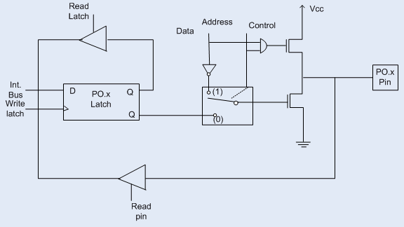
Operation
-
Input Mode:
- To configure as input, write a '1' to the corresponding latch bit.
- Both output MOSFETs are turned off, resulting in a high-impedance state.
- External devices or pull-up resistors determine the pin's voltage level.
-
Output Mode:
- Writing '0': The lower MOSFET turns on, pulling the pin to ground (logic '0').
- Writing '1':
- Both MOSFETs turn off, resulting in a high-impedance state.
- An external pull-up resistor is required to achieve a high output (logic '1').
-
External Memory Interfacing:
- A control signal (likely ALE) determines if Port 0 functions in address/data mode.
- When acting as the address/data bus:
- '0' Output: Lower MOSFET on, upper MOSFET off.
- '1' Output: Lower MOSFET off, upper MOSFET on (the bus itself will pull the line high).
Key Points
- Pull-up Resistors: Port 0 absolutely requires external pull-up resistors when used as general-purpose I/O in situations where you need to output a logic '1'.
- Versatility with Tradeoffs: The dual-functionality of Port 0 offers flexibility, but adds a layer of complexity when interfacing external memory.
Port 1 Pin Structure
-
Dedicated I/O: Port 1 is a simple 8-bit bidirectional I/O port. Its pins do not have any additional alternate functionality like serving as address lines or special control signals.
-
Internal Pull-up Resistors: A crucial feature of Port 1 is that each pin is connected to a weak internal pull-up resistor. These resistors are automatically enabled when the port pin is configured as an input.
-
Internal Diagram (Simplified):
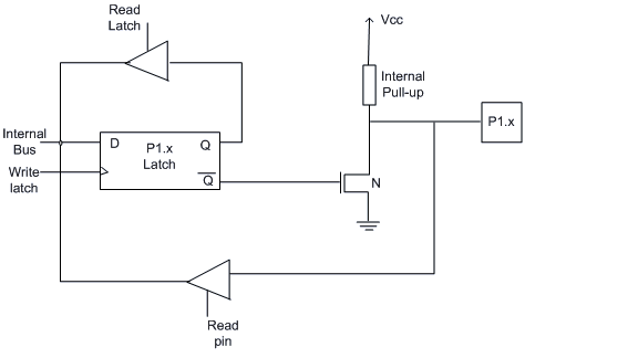
Operation
-
Input Mode:
- To configure as input, write a '1' to the corresponding latch bit.
- The internal pull-up resistor weakly pulls the pin towards a high voltage level (logic '1').
- To read a logic '0', an external device must be strong enough to overcome the internal pull-up and pull the pin to ground.
-
Output Mode:
- To configure as output, write a '0' or '1' to the corresponding latch bit.
- The internal pull-up resistor is effectively overridden.
- Writing '0': The output driver actively pulls the pin low.
- Writing '1': The output becomes high-impedance, but the internal pull-up resistor weakly pulls the pin towards a high state.
Important Considerations
- Weak Pull-ups: The internal pull-up resistors on Port 1 are relatively weak. If a connected external device attempts to strongly drive a pin low, it might not be able to fully bring the voltage to a valid logic '0' level.
- Sinking Current: When a Port 1 pin is configured as an input and an external device drives it low, the external circuitry needs to be able to sink the current flowing through the internal pull-up resistor.
- Potential for Incorrect Readings: If an external device is not strong enough or is configured incorrectly, the input may not register a true '0' even when the external device intends to drive it low.
Recommendations
- Input Considerations: If using Port 1 for inputs where strong logic '0' signals are needed, consider either:
- Disabling the internal pull-ups (if software/hardware allows it) and using external pull-down resistors.
- Using a different port without built-in pull-ups.
- Output Considerations: Port 1 can drive outputs effectively, but keep in mind that writing a '1' relies on the internal pull-up or an external pull-up to achieve the high state.
Port 2 Pin Structure
-
Dual Roles:
- Higher Order Address Bus: When the 8051 is interfaced with external memory, Port 2 provides the upper 8-bits of the 16-bit address (A8-A15).
- General Purpose I/O: If external memory is not in use, Port 2 can function as a standard 8-bit bidirectional I/O port.
-
Internal Pull-up Resistors: Similar to Port 1, each pin of Port 2 has an internal pull-up resistor that is active when the pin is configured as an input.
-
Internal Diagram (Simplified):
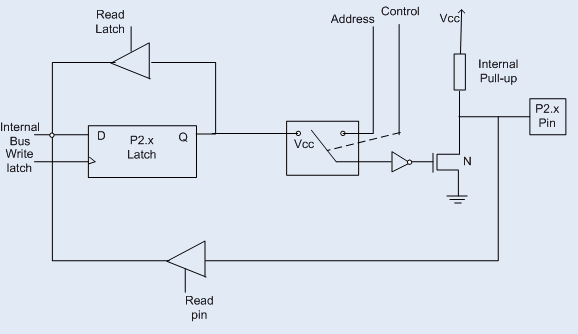
Operation
-
Input Mode:
- To configure as input, write a '1' to the corresponding latch bit.
- The internal pull-up weakly pulls the pin high (logic '1').
- External devices must be strong enough to overcome the pull-up resistor to drive a logic '0'.
-
Output Mode:
- To configure as output, write a '0' or '1' to the corresponding latch bit.
- The output driver actively drives the pin high or low, overriding the internal pull-up.
-
External Memory Interfacing:
- When used as the higher address byte, the Port 2 latch holds the address information.
- Latch values remain stable during external memory operations.
Important Considerations
- Limited Current Capacity: As with Port 1, the internal pull-ups on Port 2 mean it's not ideal for driving heavy loads or sinking significant current, especially in input mode.
- Conflict with External Memory: When using external memory, Port 2's general-purpose I/O functionality is effectively unavailable.
- Design Trade-offs: The dual-role capability of Port 2 adds flexibility, but requires careful consideration of its function in relation to other system requirements.
Recommendations
- Input Considerations: The same recommendations for Port 1 apply to Port 2. Consider external pull-down resistors or disabling the internal pull-ups if reliable '0' inputs are crucial and your external devices are weak drivers.
- External Memory Considerations: If using external memory, avoid relying on Port 2 for general-purpose inputs.
Port 3 Pin Structure
-
Multifunctional: Port 3, unlike Ports 1 and 2, is the most versatile port on the 8051. Each of its 8 pins (P3.0-P3.7) can serve either as a general-purpose I/O pin or take on a specialized alternate function.
-
Internal Pull-ups: Each pin on Port 3 has a weak internal pull-up resistor, similar to Ports 1 and 2. This pull-up is active when the pin is configured as an input.
-
Alternate Function Control:
- Latch: Each Port 3 bit has a corresponding latch bit. Writing a '1' to the latch allows the alternate function to be used.
- Priority: If multiple alternate functions compete for the same pin, a priority system exists to determine which function takes precedence.
-
Internal Diagram (Simplified):
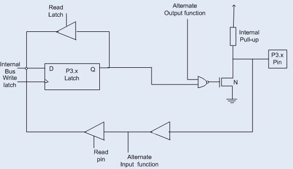
Alternate Functions of Port 3
| PORT 3 Pin | Function | Description |
|---|---|---|
| P3.0 | RXD | Serial Data Receive for UART communication. |
| P3.1 | TXD | Serial Data Transmit for UART communication. |
| P3.2 | INT0 | External Interrupt 0 input. |
| P3.3 | INT1 | External Interrupt 1 input. |
| P3.4 | T0 | Timer/Counter 0 external input. |
| P3.5 | T1 | Timer/Counter 1 external input. |
| P3.6 | WR | Write strobe for external memory. |
| P3.7 | RD | Read strobe for external memory. |
Table: Alternate Functions of Port 3
Operation
-
Input Mode:
- Write a '1' to the pin's latch bit.
- The internal pull-up pulls the pin high.
- External devices must overcome the pull-up to drive a strong logic '0'.
-
Output Mode:
- Write a '0' or '1' to the pin's latch bit.
- Output drivers actively drive the pin high or low.
-
Alternate Function Mode:
- Write a '1' to the corresponding latch bit to enable the alternate function.
- The pin is now dedicated to its special role (serial communication, interrupt, etc.).
Important Notes
- Flexibility and Tradeoffs: Port 3's versatility comes at the cost of reduced I/O capability if many alternate functions are in use.
- Configuration: Careful software configuration is essential to determine whether a Port 3 pin acts as general-purpose I/O or in its alternate function role.
Memory Organization
Program Memory (ROM)
- Purpose: The program memory is where the 8051 stores the instructions that make up the program it's executing. Think of it as the microcontroller's 'recipe book' of code.
- Types:
- Internal ROM: Most 8051 derivatives have some amount of built-in program memory (often around 4KB).
- External ROM: If a program is too large to fit in the internal ROM, the 8051 can interface with external memory chips to expand its program storage.
- Non-volatile: This means that the program code remains stored even when the 8051 loses power.
- Access Control: The external memory is accessed through the External Access (EA) pin. By default, the EA pin is connected to VCC, so the microcontroller fetches instructions from internal memory first. If the program size exceeds 4KB, the microcontroller will automatically switch to external memory. To force the microcontroller to use external memory only, connect the EA pin to GND.
Diagram (Program Memory)
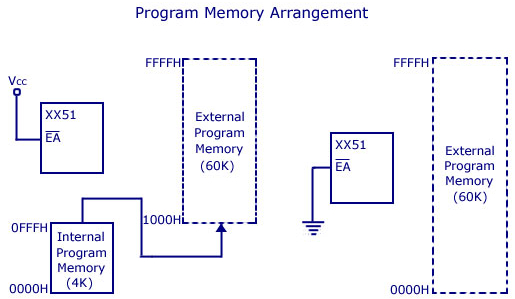
A simplified visual representation of program memory might look like this:
+--------------------+
| Program Memory (ROM)|
+--------------------+
|  Instruction 1      |
|  Instruction 2      |
|        ...          |
|  Instruction N      |
+--------------------+
Data Memory (RAM)
- Purpose: The data memory acts as the 8051's workspace. It holds temporary variables, intermediate calculations, and other data the program needs while running.
- Types
- Internal RAM: The 8051 has a limited amount of internal RAM (usually 128 bytes).
- External RAM: Like with program memory, the 8051 can utilize external RAM for additional data storage.
- Volatile: Data in RAM is lost when the 8051 loses power.
Structure of Internal Data Memory
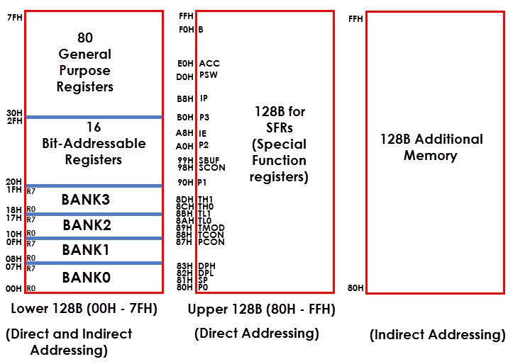
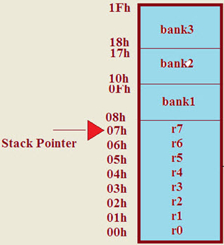
Most modern 8051 variants provide 256 bytes of internal RAM, which is organized into the following distinct areas:
1. Working Registers (00H - 1FH)
- Register Banks: The first 32 bytes of RAM are divided into four register banks (Bank 0, Bank 1, Bank 2, Bank 3). Each bank contains eight general-purpose registers (R0-R7).
- Addressing:
- By Name: Access registers by name (R0, R1, etc.) after selecting the appropriate bank using the RS0 and RS1 bits in the Program Status Word (PSW) register.
- By Address Access registers directly by their address (e.g., 12H for R2 in Bank 2), regardless of the currently selected bank.
2. Bit-Addressable Memory (20H - 2FH)
- Individual Bit Control: This area contains 128 individually addressable bits (00H - 7FH within the byte range 20H-2FH). This is efficient for storing single-bit values like flags or control signals.
3. General Purpose RAM (Scratchpad) (30H - 7FH)
- Flexible Storage: This 80-byte area provides general-purpose data storage for variables and temporary data.
- Stack: The stack, used for storing function call return addresses and temporary storage during interrupts, also resides within this area.
4. Special Function Registers (SFRs) (80H - FFH)
| Address (hex) | Register Name | Description |
|---|---|---|
| 80 | P0 | Port 0 (Input/Output) |
| 90 | P1 | Port 1 (Input/Output) |
| A0 | P2 | Port 2 (Input/Output) |
| B0 | P3 | Port 3 (Input/Output) |
| 81 | SP | Stack Pointer |
| 82 | DPL | Data Pointer Low Byte |
| 83 | DPH | Data Pointer High Byte |
| 87 | PCON | Power Control Register |
| 88 | TCON | Timer/Counter 0 Control Register |
| 89 | TMOD | Timer/Counter 0/1 Mode Register |
| 8A | TL0 | Timer/Counter 0 Low Byte |
| 8B | TL1 | Timer/Counter 1 Low Byte |
| 8C | TH0 | Timer/Counter 0 High Byte |
| 8D | TH1 | Timer/Counter 1 High Byte |
| 98 | SCON | Serial Control Register |
| 99 | SBUF | Serial Data Buffer |
| A8 | IE | Interrupt Enable Register |
| B8 | IP | Interrupt Priority Register |
| D0 | PSW | Program Status Word (contains flags) |
| E0 | ACC | Accumulator |
| F0 | B | B Register (auxiliary) |
Table: Special Function Registers (SFRs)
- Hardware Control: SFRs occupy the upper 128 bytes of RAM and directly control various hardware functions of the 8051, such as:
- I/O Ports (P0, P1, P2, P3)
- Program Status Word (PSW)
- Accumulator (A)
- Interrupt Control (IE, IP)
- Power Management (PCON)
- Direct Addressing Only: SFRs can only be accessed using their specific addresses. Unused addresses within this range are reserved and cannot be used for general-purpose data storage.
Key Points
- Indirect Addressing: The lower 128 bytes of RAM (working registers, bit-addressable area, and scratchpad) can be addressed both directly (by their address) and indirectly (using a register to hold the address).
- Limited RAM Capacity: The 8051's internal RAM is relatively small. Many applications require interfacing external RAM to support larger datasets.
- Variant Differences: Some 8051 variants may have an additional 128 bytes of RAM sharing the same address space as SFRs. This extra RAM is usually only accessible via indirect addressing.
- Speed: Internal RAM is extremely fast to access compared to external RAM, as it's located directly on the microcontroller chip.
- Flexibility: The bit-addressable area provides fine-grained control over individual bits, ideal for control and status flags.
How Internal RAM Is Used
- Arithmetic and Logical Operations: The register banks are heavily used by the ALU for arithmetic and logical operations.
- Temporary Storage: All sections of the internal RAM can be used for temporarily storing data during calculation or program execution.
- Stack: Although the 8051 has a dedicated hardware stack, the general-purpose RAM can also be used as a stack area in constrained situations.
- Flags and Control: The bit-addressable area often houses individual control flags and status bits for the 8051 or its peripherals.
Example
Assembly
External Memory Interfacing and Decoding Logic
External Memory Interfacing in the 8051
The 8051 microcontroller offers limited internal program and data memory, which might not be sufficient for complex applications. To expand its memory capacity, the 8051 can be interfaced with external memory devices like ROM and RAM. This capability allows you to store larger programs and work with more data.
Key Components Involved:
- Microcontroller: The 8051 itself, responsible for controlling data flow and program execution.
- External Memory: ROM chips for program storage and RAM chips for data storage. Both can be up to 64KB in size.
- Address Decoding Logic: Circuitry that translates the microcontroller's memory addresses into specific chip select signals for each external memory device.
- Control Signals: Signals like PSEN (Program Store Enable), RD (Read), and WR (Write) from the microcontroller to control external memory operations.
- Data Bus: A bidirectional bus that carries data between the microcontroller and external memory.
Addressing and Decoding Process:
- Memory Access Initiation: The microcontroller initiates a memory access operation, specifying an address and indicating whether it's a read or write operation.
- Address Bus Decoding: The address decoding logic receives the address from the microcontroller.
- Chip Select Generation: Based on the decoded address and the memory map, the decoding logic generates individual chip select signals for the appropriate ROM or RAM chip(s).
- Control Signal Assertion: The microcontroller asserts control signals like PSEN, RD, or WR along with the data (for write operations) onto the control and data buses.
- Data Transfer: The selected memory chip(s) perform the read or write operation based on the control signals and data provided.
- Data Bus Interaction: The data is transferred between the microcontroller and the selected memory chip(s) on the data bus.
Example:
Imagine the microcontroller wants to read data from byte address 40000 (64KB ROM, 0-31KB for ROM, 32KB-63KB for RAM) in external memory.
- The address 40000 is sent to the address decoding logic.
- The logic recognizes it's within the ROM address range (0-31KB) and generates a chip select for the ROM chip.
- The microcontroller asserts the RD (read) signal and places the address 40000 on the address bus.
- The selected ROM chip reads the data at byte address 40000 and places it on the data bus.
- The microcontroller reads the data from the data bus and stores it internally.
The below image shows a simplified block diagram of interfacing 64KB ROM and 64KB RAM with the 8051:
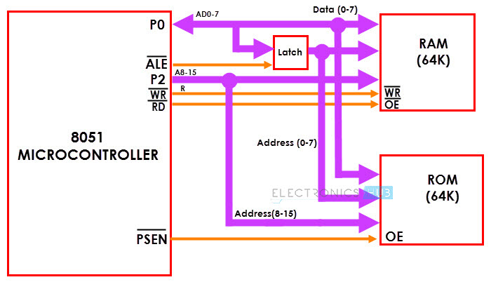
- Microcontroller: Represented by the 8051 block.
- External Memory: ROM and RAM blocks labeled as "64K ROM" and "64K RAM".
- Address Decoding Logic: Not explicitly shown but implied by the connections between the address bus and chip select signals.
- Control Signals: PSEN, RD, and WR signals are shown from the microcontroller.
- Data Bus: Represented by the bidirectional "Data (0-7)" lines.
Stack, Stack Pointer, and Stack Operations
What is the Stack?
- LIFO Structure: The stack is a section of the 8051's internal RAM that follows a Last-In, First-Out (LIFO) principle. Imagine it like a stack of plates; you always add and remove from the top.
- Purpose:
- Temporary Storage: The stack stores data temporarily during program execution.
- Function Calls: It saves the return address when a function (subroutine) is called, allowing the program to return to the correct point after the function completes.
- Interrupts: When an interrupt occurs, the 8051 temporarily pushes the current program counter (PC) onto the stack, allowing it to later resume execution where it was interrupted.
Stack Pointer (SP)
- Address Tracker: The Stack Pointer (SP) is an 8-bit register that holds the address of the top of the stack (the last item added).
- Initialization: Upon reset, the SP is usually initialized to 07H within the 8051's internal RAM.
- Dynamic: The SP changes automatically during stack operations (push and pop).
Stack Operations
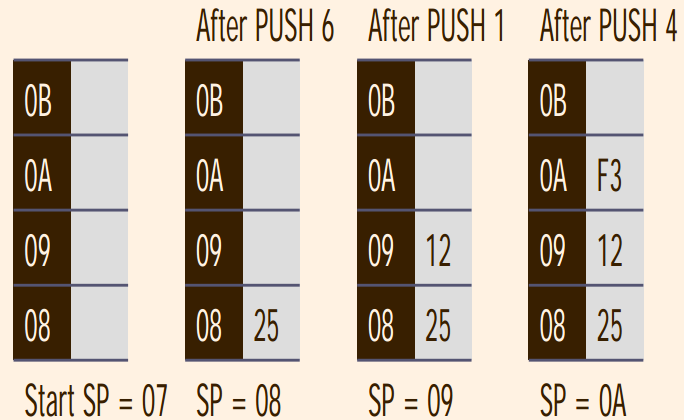
- PUSH Instruction:
- Stores Data: The PUSH instruction puts a byte of data onto the top of the stack.
- SP Modification:
- The SP is incremented.
- The data is then stored at the memory location now pointed to by the SP.
PUSH Example:
Assembly
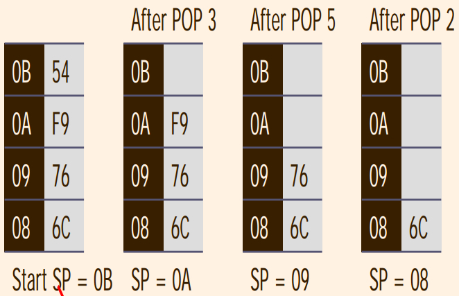
- POP Instruction:
- Retrieves Data: The POP instruction removes a byte of data from the top of the stack.
- SP Modification:
- The data at the location pointed to by the SP is retrieved.
- The SP is then decremented.
POP Example:
Assembly
Common Uses of the Stack
-
Temporary Storage: Storing the contents of registers during calculations when there aren't enough registers available.
-
Subroutine Calls: When a subroutine (function) is called using the 'CALL' instruction, the return address (next instruction after the call) is automatically pushed onto the stack. The 'RET' instruction pops this return address, so execution continues correctly.
-
Interrupt Handling: When an interrupt occurs, the 8051 automatically pushes the Program Counter (PC) onto the stack, allowing seamless return to the interrupted code after the interrupt service routine.
Important Considerations
- Limited Stack Size: The 8051's internal RAM is small, which limits the size of the stack. Be mindful of stack usage to avoid overflow conditions.
- Stack Overflow: This occurs if you try to PUSH data when the stack is full. This can lead to unpredictable behavior.
- Stack Underflow: This occurs if you try to POP data when the stack is empty. This can also result in errors.
- Stack Size: The 8051's internal RAM for the stack is limited; it's crucial to prevent stack overflow.
- Initialization: The SP is initialized to 07H when the 8051 resets; your code often needs to set it to a custom location.
Example: Swapping Two Numbers
Assembly
Timers/Counters
8051 Timers/Counters have two primary modes of operation:
- Timer Mode:
- Increments on internal machine cycles.
- Used to generate time delays or measure time intervals between events.
- Counter Mode:
- Increments on external pulses applied to designated input pins.
- Used to count external events, like sensor inputs or rotations of a shaft.
Structure
- Two Timers/Counters: The 8051 has two flexible 16-bit timers/counters, named Timer 0 and Timer 1.
- Registers: Each timer/counter has the following registers:
- THx and TLx: "x" denotes the timer number – Timer 0 (TH0, TL0) and Timer 1 (TH1, TL1). These hold the actual timer/counter values.
- TMOD: The Timer Mode register (configuration of modes).
- TCON: The Timer Control register (start, stop, interrupt flags, etc.).
Applications
- Timing and Delays: Generating precise delays in code.
- Event Counting: Counting occurrences of external events (button presses, sensor triggers, etc.).
- PWM (Pulse-Width Modulation): Used to control the speed of motors, brightness of LEDs, etc.
- Baud Rate Generation: Essential for serial communication in the 8051.
- Real-Time Clock (RTC): Along with external circuitry, Timers can be used to implement an RTC.
Limitations
- ReSolution:**** Limited by the 8051's clock speed and the timer/counter's 16-bit design. Fine-grained timings and very high-frequency counting may be difficult.
- Only Two Timers: Some complex applications might require more than the two timers the 8051 provides.
TCON Register
What is the TCON Register?
- The TCON (Timer Control) register is an 8-bit, bit-addressable register present in 8051 microcontrollers.
- It's primarily responsible for controlling the operation of the microcontroller's internal timers and counters.
TCON Register Structure (Address: 088H, Bit addressable)
| TCON.7 | TCON.6 | TCON.5 | TCON.4 | TCON.3 | TCON.2 | TCON.1 | TCON.0 |
|---|---|---|---|---|---|---|---|
| TF1 | TR1 | TF0 | TR0 | IE1 | IT1 | IE0 | IT0 |
Table: TCON Register Structure
The 8 bits of the TCON register are assigned specific functions:
- TF1 (Timer 1 Overflow Flag): Set to '1' when Timer 1 overflows. Cleared by software.
- TR1 (Timer 1 Run Control Bit): Controls the Run/Stop status of Timer 1.
- '1' = Timer 1 is running
- '0' = Timer 1 is stopped
- TF0 (Timer 0 Overflow Flag): Set to '1' when Timer 0 overflows. Cleared by software.
- TR0 (Timer 0 Run Control Bit): Controls the Run/Stop status of Timer 0.
- '1' = Timer 0 is running
- '0' = Timer 0 is stopped
- IE1 (External Interrupt 1 Edge Flag): Set to '1' when an external interrupt 1 occurs on a falling edge transition. Cleared by software.
- IT1 (External Interrupt 1 Type Control Bit): Configures external interrupt 1 trigger type.
- '1' = Falling edge triggered
- '0' = Low-level triggered.
- IE0 (External Interrupt 0 Edge Flag): Set to '1' when an external interrupt 0 occurs on a falling edge transition. Cleared by software.
- IT0 (External Interrupt 0 Type Control Bit): Configures external interrupt 0 trigger type.
- '1' = Falling edge triggered
- '0' = Low-level triggered
| Flag | Function |
|---|---|
| TF1 | Timer 1 Overflow flag. Set when timer rolls from all 1's to 0. Cleared when processor vectors to execute interrupt service routine located at program address 001Bh. |
| TR1 | Timer 1 run control bit. Set to 1 by program to enable timer to count; cleared to 0 by program to halt timer. |
| TF0 | Timer 0 Overflow flag. Set when timer rolls from all 1's to 0. Cleared when processor vectors to execute interrupt service routine located at program address 000Bh. |
| TR0 | Timer 0 run control bit. Set to 1 by program to enable timer to count; cleared to 0 by program to halt timer. |
| IE1 | External interrupt 1 Edge flag. Set to 1 when a high-to-low edge signal is received on port 3.3 (INT1). Cleared when processor vectors to interrupt service routine at program address 0013h. Not related to timer operations. |
| IT1 | External interrupt 1 signal type control bit. Set to 1 by program to enable external interrupt 1 to be triggered by a falling edge signal. Set to 0 by program to enable a low-level signal on external interrupt 1 to generate an interrupt. |
| IE0 | External interrupt 0 Edge flag. Set to 1 when a high-to-low edge signal is received on port 3.2 (INT0). Cleared when processor vectors to interrupt service routine at program address 0003h. Not related to timer operations. |
| IT0 | External interrupt 0 signal type control bit. Set to 1 by program to enable external interrupt 1 to be triggered by a falling edge signal. Set to 0 by program to enable a low-level signal on external interrupt 0 to generate an interrupt. |
Table: TCON Register Function
Key Functions of TCON Register
-
Timer/Counter Start/Stop: The TR1 and TR0 bits enable you to start and stop Timer 1 and Timer 0, respectively.
-
Overflow Monitoring: The overflow flags TF1 and TF0 indicate when a timer has reached its maximum count and rolled over. These are often used to generate interrupts.
-
External Interrupt Configuration: The IE0, IT0, IE1, and IT1 bits control how external interrupts are triggered and detected by the microcontroller.
Example: Setting up Timer 0 as an interval timer
-
Set the Mode: To use Timer 0 in a specific mode, you'll configure the TMOD register (Timer Mode Register). Let's assume you want Timer 0 as a 16-bit interval timer.
-
Load Initial Value: Load the desired starting count into the TH0 (Timer 0 High Byte) and TL0 (Timer 0 Low Byte) registers.
-
Start the Timer: Set TR0 (Timer 0 Run Control Bit) in the TCON register to '1' to begin the timer.
-
Interrupt Handling (Optional): If you want an interrupt to be generated when the timer overflows, set the interrupt enable bits in relevant registers and create an interrupt service routine (ISR). The TF0 flag in TCON will be set when an overflow occurs.
TMOD Register
What is the TMOD Register?
- The TMOD (Timer Mode) register is an 8-bit, bit-addressable Special Function Register (SFR) within 8051 microcontrollers.
- Its primary role is to select and configure the operating modes of the two built-in timers: Timer 0 and Timer 1.
TMOD Register Structure (Address: 089H, Bit addressable):
| TMOD.7 | TMOD.6 | TMOD.5 | TMOD.4 | TMOD.3 | TMOD.2 | TMOD.1 | TMOD.0 |
|---|---|---|---|---|---|---|---|
| Timer1 GATE | Timer1 C/T | Timer1 M1 | Timer1 M0 | Timer0 GATE | Timer0 C/T | Timer0 M1 | Timer0 M0 |
Table: TMOD Register Structure
The TMOD register has a specific function assigned to each of its 8 bits:
- Bits 7-4 (Timer 1 Configuration)
- Gate: Controls Timer 1 gating for external control (described later).
- C/T: Selects Timer vs. Counter mode for Timer 1.
- '1' = Counter mode (counts external pulses)
- '0' = Timer mode (counts internal machine cycles)
- M1 M0: Selects the operating mode of Timer 1 (Modes 0, 1, 2, or 3)
- Bits 3-0 (Timer 0 Configuration): Same structure as Timer 1 configuration bits above, but control the settings for Timer 0.
| Bit | Function |
|---|---|
| Timer1 GATE | GATE enables and disables Timer by means of a signal brought to the INTx pin: 1 – Timer operates only if the INTx bit is set. 0 – Timer operates regardless of the logic state of the INTx bit. |
| Timer1 C/T | C/T selects pulses to be counted up by the timer/counter: 1 – Timer counts pulses brought to the Tx(Timer) pin. 0 – Timer counts pulses from the internal oscillator. |
| Timer1 M1 | M1, M0 These two bits select the operational mode Timer. |
| Timer1 M0 | M1, M0 These two bits select the operational mode Timer. |
| Timer0 GATE | GATE enables and disables Timer by means of a signal brought to the INTx pin: 1 – Timer operates only if the INTx bit is set. 0 – Timer operates regardless of the logic state of the INTx bit. |
| Timer0 C/T | C/T selects pulses to be counted up by the timer/counter: 1 – Timer counts pulses brought to the Tx(Timer) pin. 0 – Timer counts pulses from the internal oscillator. |
| Timer0 M1 | M1, M0 These two bits select the operational mode Timer. |
| Timer0 M0 | M1, M0 These two bits select the operational mode Timer. |
Table: TMOD Register Function
Operating Modes
| M1 | M0 | Mode | Operating Mode |
|---|---|---|---|
| 0 | 0 | 0 | 13-bit Mode |
| 0 | 1 | 1 | 16-bit Mode |
| 1 | 0 | 2 | 8-bit Auto Reaload Mode |
| 1 | 1 | 3 | Split Timer Mode |
Table: Timer Operating Modes Selection
The TMOD register allows you to configure each timer into one of four operating modes:
- Mode 0 (13-bit Timer):
- Timer register is effectively 13 bits (THx: 8 bits, TLx: 5 bits)
- This mode is often used for simple timing or event counting where extremely long delays are not required.
- Mode 1 (16-bit Timer):
- The standard 16-bit timer/counter mode, providing the full range of counting.
- Mode 2 (8-bit Auto-Reload Timer):
- TLx is reloaded with the value in THx automatically after each overflow. Useful for generating fixed periodic events.
- Mode 3 (Split Timer):
- Timer 1 is stopped. TL0 is used as an 8-bit Timer/Counter and can be controlled independently, while TH0 runs as a separate 8-bit timer (usually controlled by the system clock).
Gate Bit
The Gate bit for each timer provides additional control:
- Gate = '0': The timer runs continuously when the TRx bit (in TCON) is set to '1'.
- Gate = '1': The timer runs only when the TRx bit is '1' AND an external pin (INT0 or INT1) receives a high-to-low transition.
Example: Configuring Timer 0 as a 16-bit timer with gating
-
Setting the Mode: To configure Timer 0 as a 16-bit timer, set the corresponding bits in the TMOD register as follows:
TMOD = 0x01; // Assuming you want Timer 0 in Mode 1, Timer 1 is not important here -
Enabling Gating: If you want to control Timer 0 with an external signal on INT0 pin:
TMOD |= 0x08; // Set the Gate bit for Timer 0
Modes of Operation
Mode 0: 13-Bit Timer
- Configuration: The timer register is split into two parts:
- Five high-order bits (THx)
- Eight low-order bits (TLx), with the top 3 bits of TLx written as zeroes.
- Operation: The 5 bits of TLx are automatically incremented. When TLx overflows, it increments THx. This forms a 13-bit timer.
- Use Cases: Often used for event counting or generating baud rates in serial communication, particularly when interfacing with legacy systems.
Mode 1: 16-Bit Timer
- Configuration: The full 16-bits of the Timer register (THx and TLx) function as a single timer unit.
- Operation: Each clock pulse increments the entire register.
- Use Cases General-purpose time delays, long interval measurements, anything requiring 16-bit precision timing.
Mode 2: 8-Bit Auto-Reload Timer
- Configuration:
- THx holds a fixed reload value.
- TLx operates as the 8-bit timer.
- Operation:
- TLx counts up. When it overflows, it's automatically reloaded with the value stored in THx.
- This creates a recurring time interval.
- Use Cases: Generating fixed, predictable time delays or timing periodic events.
Mode 3: Split 8-bit Timers
- Configuration:
- Timer 0 is split into two independent 8-bit timers/counters: TL0 and TH0.
- Timer 1 remains as a 16-bit timer if needed.
- Operation:
- TL0 and TH0 function as two separate timers, often with TL0 used as a timer and TH0 used as a counter.
- Use Cases:
- Situations requiring two independent timers
- Generating baud rates (TL0) while counting external events (TH0)
Key Control Registers
- TMOD (Timer Mode): This register selects the operating mode for Timer 0 and Timer 1.
- TCON (Timer Control): Contains flags and start/stop control bits for the timers.
How to Select a Mode
Mode selection depends on:
- Timing Precision: 16-bit vs. 8-bit
- Recurring Intervals: Auto-reload mode vs. manual restart.
- Number of Timers Needed: Split timer mode provides two independent 8-bit timers if needed within Timer 0.
Timer Mode 0 (13-bit Timer Mode)
- Split Registers: In Mode 0, each timer's 16-bit register is effectively split into:
- THx (8 bits): Holds the upper 8 bits of the timer count.
- TLx (5 bits): Holds the lower 5 bits of the timer count.
- Counter Behavior: Only TLx is actually incremented. Whenever TLx overflows (reaches 32 counts), it's reset to zero, and THx is incremented by one.
- Effective Count: This provides a 13-bit count. The maximum count is effectively 8192 (2^13).
Key Points about Mode 0
- Timer vs. Counter: Mode 0 can be used as either a timer (counting internal machine cycles) or as a counter (counting external pulses). This is controlled by the C/T bit in the TMOD register.
- Limited Range: Due to the 13-bit design, Mode 0 is primarily useful for relatively short delays or event counting where extremely long intervals are not required.

Example: Creating a Delay Using Timer 0 in Mode 0
Assuming you have a 12 MHz crystal oscillator for your 8051 (1 machine cycle = 1 microsecond):
-
Mode Setup:
C -
Calculate Delay Value:
- Let's say you want a 50-millisecond (0.05 seconds) delay.
- We need 50000 machine cycles (50,000 microseconds).
- Because the timer counts up, calculate the value to subtract from the max value: 8192 - 50000 = -41808.
- Since the counter is unsigned, the 16-bit representation of -41808 is 3CAF (hex).
-
Load Timer Registers:
C -
Start Timer:
C -
Wait for Overflow:
C
Explanation
The timer will start counting up from 0x3CAF. After 41808 machine cycles, an overflow will occur, setting TF0 to '1'. Your code detects this and stops the timer. You have now generated your desired 50-millisecond delay.
Timer Mode 1 (16-bit Timer Mode)
- Full 16-bit Register: In Mode 1, both THx and TLx registers of a timer act as a single 16-bit register.
- Counting: The 16-bit register is incremented on each timer pulse (either internal machine cycles or external pulses, depending on the C/T bit in TMOD).
- Maximum Count: Timers in Mode 1 can count up to the full 16-bit range, which is 65,536.

Example: Generating a 1-Second Delay with Timer 0 in Mode 1
Let's assume a 12 MHz crystal oscillator (1 machine cycle = 1 microsecond):
-
Mode Setup:
Assembly -
Calculating the Reload Value:
- We need a 1-second delay (1,000,000 microseconds).
- Since the timer increments on each machine cycle, we need 1,000,000 counts.
- To create a delay, we subtract this from the max count and load the result: 65536 - 1000000 = -934464
- As the counter is unsigned, the 16-bit representation is FC18 (hex).
-
Loading Timer Registers:
Assembly -
Starting the Timer:
Assembly -
Waiting for Overflow:
Assembly
Explanation
- The timer starts counting from FC18. When it reaches FFFF, it overflows, setting the TF0 flag to '1'.
- The
JNB TF0, $instruction creates a loop that checks the TF0 flag, effectively waiting for the overflow. - Once the overflow occurs, the timer is stopped, and the flag is cleared.
Important Notes:
- The C/T bit in the TMOD register determines whether the timer counts internal machine cycles (timer mode) or external pulses (counter mode).
- Mode 1 is the most common mode for timers in 8051 microcontrollers due to its flexibility and larger counting range.
Timer Mode 2 (8-bit Auto-Reload Timer Mode)
- Key Feature: In Mode 2, the TLx register acts as the timer itself, while the THx register holds a reload value.
- Auto-Reload Behavior:
- TLx counts up.
- When TLx overflows from FFH to 00H, it's automatically reloaded with the value stored in THx.
- This cycle repeats, generating a continuous timer.
Advantages of Mode 2
- Fixed-Period Generation: Mode 2 is ideal for generating fixed-period delays or timing events without requiring software intervention to reload the timer after each cycle.
- Baud Rate Generation: Mode 2 is often used in serial communication to create a reliable clock for baud rate generation.

Example: Creating a Square Wave with 50% Duty Cycle on Timer 1
Assumptions:
- 12 MHz crystal oscillator.
- Desired square wave frequency: 1 kHz (period = 1 millisecond).
-
Mode Setup:
Assembly -
Calculating Reload Value:
- A 1 kHz wave with a 50% duty cycle requires a 0.5 millisecond on-time and a 0.5 millisecond off-time.
- 0.5 ms corresponds to 6000 machine cycles (0.5 ms * 12,000 cycles/ms).
- To make the timer count for 6000 cycles, we need to load the reload value with 256 - 6000 = -5744.
- The 8-bit representation of -5744 is DAH (hex).
-
Loading TH1:
Assembly -
Starting the Timer:
Assembly -
Generating the Square Wave (Hardware handles most of this):
- Connect an output pin of your microcontroller to the T1 pin (P3.4) for the 8051.
Explanation
- Timer 1 will begin counting up from 00H. When it reaches FFH, it overflows, automatically reloads with DAH from TH1, and the process repeats.
- The hardware of the 8051 will automatically toggle the T1 pin on each overflow, creating the square wave output.
Important Notes
- Mode 2 is exclusively a timer mode – it always counts internal machine cycles.
- You can adjust the duty cycle of the square wave in the example by changing the reload value loaded into TH1.
Timer Mode 3 (Split Timer Mode)
Mode 3 is a unique mode for Timer 0 and Timer 1 with specific behaviors:
Timer 0 in Mode 3
- TL0 (8-bit Timer/Counter): Behaves as a standard 8-bit timer or counter, controlled by the C/T bit in TMOD and the TR0 bit in TCON.
- TH0 (8-bit Timer): Acts as an independent timer, usually controlled by the system clock (machine cycles). It is not affected by TR0 in this mode.
Timer 1 in Mode 3
- Stopped: Timer 1 is essentially halted in Mode 3.
- Control Bits: Timer 1's control bits (TR1 and TF1) are used instead by Timer 0. This allows Timer 0 to be gated (controlled by an external signal).
Why is Mode 3 Useful?
- Extra Timer: Mode 3 gives you an additional 8-bit timer (TH0) if you need more than the standard two timers that the 8051 provides.
- Gating Timer 0: It allows you to control the Start/Stop of Timer 0 with an external signal on the INT0 pin, providing more flexible control for timing operations.

Example: Using Timer 0 in Mode 3 as a Gated Timer
Let's assume you want Timer 0 to count external events on pin INT0 and TH0 to generate a time base.
-
Mode Setup:
Assembly -
Gating Setup:
Assembly -
Using the Functionality
- TL0: Will now count pulses received on the INT0 pin.
- TH0: Will count machine cycles and can be used for independent timing operations.
- To start Timer 0: Ensure TR0 is set to '1' AND a high-to-low transition occurs on the INT0 pin.
Key Points
- Mode 3 for Timer 1 is rarely used directly; its primary purpose is to give Timer 0 the extra control features.
- Timer 0 needs both TR0 = '1' and the external gating signal for it to function when in Mode 3.
Serial Communication
What is Serial Communication?
- Serial communication is a method of transmitting data between devices where the bits of data are sent sequentially over a single communication line or channel. This contrasts with parallel communication where multiple bits are sent at the same time over multiple lines.
Key Modes of Serial Communication
-
Simplex Mode
- Unidirectional transmission: Data flows in only one direction, from the transmitter to the receiver.
- Example: A TV broadcasting station transmits signals to countless television sets (receivers). TVs can't transmit back to the station.
-
Half-Duplex Mode
- Bidirectional, but not simultaneous: Both devices can transmit and receive, but not at the same time. They must take turns.
- Example: Walkie-talkies. A user presses a button to talk (transmit) and releases the button to listen (receive). Both users cannot talk at the same time.
-
Full-Duplex Mode
- Simultaneous bidirectional transmission: Both devices can transmit and receive data at the same time.
- Example: Modern phone calls. Both parties can talk and listen simultaneously.
Asynchronous vs. Synchronous Communication
Within serial communication, there's an important distinction between asynchronous and synchronous modes:
-
Asynchronous:
- No shared clock signal between devices.
- Data is framed using start and stop bits to signal the beginning and end of a data packet.
- Good for irregular data transmission with potential gaps between bytes.
-
Synchronous:
- Devices share a clock signal that synchronizes the timing of data transmission.
- Data bytes flow in a continuous stream without the need for start and stop bits.
- Ideal for high-speed, continuous data transmission.
Example: UART Communication (Typically Asynchronous)
- Hardware: A Universal Asynchronous Receiver/Transmitter (UART) is a common hardware component for serial communication.
- Protocol: Data is framed with a start bit, 5-9 data bits, an optional parity bit (for error checking), and one or more stop bits.
- Transmission:
- The transmitter sends out the start bit (logic low)
- Data bits are sent one by one (least significant bit first)
- Parity bit (if used) is sent
- Stop bit (logic high) signals packet's end
- Example Use Case: Computer sending commands to a microcontroller over a serial connection.
Note: Other serial protocols exist, such as SPI (Serial Peripheral Interface) and I2C (Inter-Integrated Circuit), each with specific features and applications.
SCON Register
What is the SCON Register?
- The SCON (Serial Control) register is an 8-bit, bit-addressable Special Function Register (SFR) responsible for managing serial communication in 8051 microcontrollers.
- It holds settings and status flags that control how the microcontroller sends and receives data serially.
SCON Register Structure (Address: 098H, Bit addressable):
| SCON.7 | SCON.6 | SCON.5 | SCON.4 | SCON.3 | SCON.2 | SCON.1 | SCON.0 |
|---|---|---|---|---|---|---|---|
| SM0 | SM1 | SM2 | REN | TB8 | RB8 | TI | RI |
Table: SCON Register Structure
Here's how the SCON register's bits function:
-
SM0, SM1 (Serial Mode Selection Bits): These bits define the serial communication mode for the 8051. There are four primary modes:
- Mode 0: 8-bit shift register for serial port output, clock for serial port input is generated internally.
- Mode 1: 10-bit UART mode (8 data bits, 1 start bit, 1 stop bit).
- Mode 2: 11-bit UART mode (8 data bits, 1 start bit, 1 programmable stop bit, 1 additional bit for addressing or other purposes)
- Mode 3: Similar to mode 2, but with 9 data bits.
SMO SM1 Mode Baud Rate Description 0 0 Mode 0 Fixed Baud Rate (fosc/12) 8-Bit Synchronous Shift Register Mode 0 1 Mode 1 Variable Baud Rate (Can be set by Timer 1) 8-bit Standard UART mode 1 0 Mode 2 Fixed Baud Rate (fosc/64) or (fosc/32) 9-bit Multiprocessor Comm. mode 1 1 Mode 3 Variable Baud Rate (Can be set by Timer 1) 9-bit Multiprocessor Comm. mode Table: Serial Mode Selection
-
SM2 (Enable Multiprocessor Communication): Specifically designed for multiprocessor systems to distinguish between data from other processors and address information.
-
REN (Receive Enable):
- '1' = Enables serial reception
- '0' = Disables serial reception.
-
TB8 (Transmit Bit 8): In Modes 2 and 3, this is the 9th data bit that is transmitted.
-
RB8 (Receive Bit 8): There are two interpretations:
- Modes 1, 2, and 3: This is the 9th data bit received.
- Mode 0: RB8 becomes the stop bit when received.
-
TI (Transmit Interrupt Flag):
- '1' = Signals that the transmit buffer is empty, ready for new data (set by hardware).
- '0' = Transmission is in progress (cleared by software).
-
RI (Receive Interrupt Flag):
- '1' = Signals that the receive buffer is full (set by hardware).
- '0' = No data in the buffer to be read (cleared by software).
| Bit | Function |
|---|---|
| SM0 | These 2 bits determine the framing of data by specifying number of bits per |
| SM1 | character and start and stop bits. they take following combo.SM0 |
| SM2 | This enables multiprocessing capabilities of 8051. Usually set to 0 |
| REN | Also referred to as SCON.4 as SCON is a bit addressable register. This is receive enable. When high or 1 it allows 8051 to receive data from RxD pin. Used or access as SET SCON.4 and CLR SCON.4. very useful in blocking external serial reception. |
| TB8 | Transfer bit 8. Used for serial mode 2 and 3 not generally used so set it always to 0 |
| RB8 | Receive bit 8. Again used for serial mode 2 and 3 not used so set it to 0 |
| TI | Transmit interrupt. Important flag bit in SCON register. When 8051 finishes transfer of 8 bit character, it raises the T1 flag to indicate that it is ready to transfer another byte. Is used at beginning of stop bit. |
| RI | Receive interrupt. Another important flag bit in SCON register. When 8051 finishes receiving data i.e when data is successfully stored in SBUF it raises R1 flag to indicate byte is received and to be picked before it gets lost. |
Table: SCON Register Function
Example: Setting up Serial Communication in Mode 1 (10-bit UART)
-
Mode Selection: Set the SM0 and SM1 bits in the SCON register:
SCON = 0x50; // Mode 1: 10-bit UART, Receiver Enabled -
Baud Rate Calculation: Determine the desired baud rate and calculate the appropriate reload value for the TH1 register (which acts as the baud rate generator). Consult your 8051 microcontroller datasheet for the calculation formula.
-
Enabling Reception (if needed): Set the REN bit in SCON to '1' to enable incoming serial data reception.
-
Transmitting Data:
- Wait for the TI flag in SCON to become '1' (meaning the transmit buffer is empty).
- Load the data byte to be transmitted into the SBUF register. The hardware handles the rest for you.
Note: To receive data, you'll usually create an interrupt service routine (ISR) that triggers when the RI flag in SCON is set.
Modes
The SCON Register's Role
The SCON (Serial Control) register holds bits that determine the operating mode, baud rate, and other serial communication settings for the 8051's integrated UART. The pertinent bits are:
- SM0, SM1: Serial Mode selection bits.
- REN: Receive enable bit.
Serial Modes in 8051
The 8051 supports four primary serial communication modes, as outlined below:
1. Mode 0 (Shift Register Mode)
- Synchronous: Data is transmitted and received with clock pulses generated on the TxD pin (transmit data pin) of the 8051. RxD (receive data pin) is used for receiving data.
- Framing: Data transmission occurs in bytes (8-bit frames) without the overhead of start and stop bits.
- Baud Rate: Fixed at 1/12th of the microcontroller's oscillator frequency.
2. Mode 1 (10-bit UART)
- Asynchronous: No shared clock signal between devices. Start and stop bits frame each byte for synchronization.
- Framing: 1 start bit, 8 data bits, and 1 stop bit.
- Baud Rate: Variable, usually determined by using Timer 1 to generate the baud-rate ticks.
- Common Use: General-purpose serial communication with external devices.
3. Mode 2 (11-bit UART)
- Asynchronous: Same principle as Mode 1.
- Framing: 1 start bit, 8 data bits, a programmable 9th bit, and 1 stop bit.
- 9th Bit: Can be used as an extra data bit, a parity bit (for error checking), or for multiprocessor communication.
- Baud Rate: Variable, often calculated using Timer 1.
4. Mode 3 (9-bit UART)
- Similar to Mode 2: Asynchronous with a programmable 9th bit.
- Framing: 1 start bit, 8 data bits, and 1 stop bit.
- Key Difference: The 9th bit is always transmitted as '1'.
- Baud Rate: Variable, based on calculations with Timer 1.
Mode Selection & Configuration Example
Let's configure the 8051 for serial communication in Mode 1, a classic UART setup:
-
Mode Setting:
C -
Baud Rate Calculation: Determine the desired baud rate and calculate the appropriate reload value to load into the TH1 register used as the baud rate generator. (Consult your microcontroller datasheet for the calculation formula).
Remember:
- To transmit data, load the byte to be sent into the SBUF (Serial Buffer) register. Hardware handles the rest.
- Reception often involves setting up interrupts to detect when the RI flag in SCON is set, indicating received data.
Mode 0 Serial Communication (Synchronous Shift Register Mode)
- Clocking: In Mode 0, the 8051 generates clock pulses on its TxD (transmit data) pin. These clock pulses synchronize data transmission and reception. The RxD (receive data) pin is used to receive incoming data.
- No Start/Stop Bits: Data is transmitted as a continuous stream of bytes (8 bits) without framing overhead like start and stop bits.
- Half-Duplex: Data can flow in either direction, but not simultaneously. Devices need to take turns transmitting and receiving.
- Fixed Baud Rate: The baud rate is fixed at 1/12th of the microcontroller's oscillator frequency.
Example: Transmitting Data to a Shift Register
A common use case for Mode 0 is communicating with external shift registers to control displays or expand I/O (input/output) capability. Let's assume:
- 12 MHz crystal oscillator (1 machine cycle = 1 microsecond)
- Sending a byte of data to a shift register
-
Mode Setup:
Assembly -
Load Data to Send:
Assembly -
Transmit Byte (Hardware Handles the Bit Shifting):
- The hardware will automatically shift out the 8 bits of data on the TxD pin, synchronized with clock pulses. The shift register will receive one bit on each clock pulse.
-
Enable Reception (If Needed):
Assembly
Key Points
- Synchronization: The external device must be designed to shift data in sync with the clock signal provided by the 8051.
- Baud Rate Limitation: The fixed baud rate (oscillator frequency / 12) may be a constraint for applications requiring high-speed communication.
Additional Considerations
- For bidirectional communication, you'll need to manage transitions between transmitting and receiving data.
- Mode 0 is less common in modern applications where UART-based asynchronous communication (Modes 1, 2, and 3) is often preferred for its flexibility.
Mode 1 Serial Communication (10-bit UART Mode)
- Asynchronous: No shared clock signal between devices. Start and stop bits frame each byte for synchronization.
- Framing:
- 1 start bit (always '0')
- 8 data bits (least significant bit sent first)
- 1 stop bit (always '1')
- Variable Baud Rate: The baud rate is often calculated using Timer 1.
- Common Use: General-purpose serial communication with external devices (sensors, Bluetooth modules, GPS modules, other microcontrollers, etc.).
Example: Transmitting and Receiving Data to/from a Computer
Let's imagine you want to send the character 'A' to your computer and then receive a character back.
Assumptions:
- 11.0592 MHz oscillator
- Desired baud rate: 9600
-
Mode Setup:
Assembly -
Baud Rate Setup (Using Timer 1):
- Use your microcontroller datasheet's calculations to determine the reload value for the TH1 register to achieve a 9600 baud rate.
- Let's say the calculated reload value is FD (hex). Load TH1 with this value.
- Set the appropriate bits in TMOD to run Timer 1 as the baud rate generator.
- Start Timer 1 by setting TR1 = 1 in the TCON register.
-
Transmitting the Character 'A' (ASCII 41H):
Assembly -
Receiving a Character:
Assembly
Explanation
- Sending: The 8051 UART hardware frames the 'A' with start/stop bits and handles the bit shifting. The TI flag is set when the byte is completely sent.
- Receiving: The hardware detects the start bit of an incoming byte, assembles it, and puts it in the SBUF register. The RI flag is set. Your code then reads the byte from SBUF.
Important Points
- Mode 1 is the most common UART mode used in 8051 systems due to its flexibility and asynchronous nature.
- You'll often handle serial communication using interrupts (signaled by TI and RI) to make your code more responsive.
Mode 2 Serial Communication (11-bit UART Mode)
- Asynchronous: Similar to Mode 1, there's no shared clock signal between devices, and start and stop bits frame each data transmission.
- Framing:
- 1 start bit (always '0')
- 8 data bits (least significant bit sent first)
- A programmable 9th bit (set by the TB8 bit in the SCON register)
- 1 stop bit (always '1')
- Variable Baud Rate: Typically calculated using Timer 1.
Key Uses of Mode 2
-
Extra Data or Parity Bit: The 9th bit can be:
- An extra data bit for sending 9-bit values.
- A configurable parity bit for error checking.
-
Multiprocessor Communication: In multiprocessor systems, the 9th bit is used by the SM2 bit in SCON to distinguish between data from other processors and address information.
Example: Transmitting Data with a Parity Bit
Let's assume you want to send the byte 'B' (ASCII 42H) with even parity.
Assumptions:
- 11.0592 MHz oscillator
- Desired baud rate: 9600
-
Mode Setup
Assembly -
Baud Rate Setup (Similar to Mode 1):
- Calculate the reload value for TH1 to achieve a 9600 baud rate (consult your datasheet).
- Load TH1 with the calculated value.
- Set up Timer 1 as the baud rate generator in TMOD.
- Start Timer 1 (TR1 = 1 in TCON).
-
Calculate Even Parity and Set TB8:
Assembly -
Transmitting
Assembly
Explanation
- Parity: Your code would calculate the even parity bit before transmission and set the TB8 bit accordingly.
- Hardware: The hardware handles framing the byte with start, stop, and parity bits.
Important Notes
- Mode 2 offers flexibility for either parity checking or transmitting 9-bit data.
- The multiprocessor communication feature is specialized and may not be relevant to most applications.
Mode 3 Serial Communication (9-bit UART Mode)
- Asynchronous: Similar to Modes 1 and 2: no shared clock signal, start and stop bits for framing.
- Framing:
- 1 start bit (always '0')
- 8 data bits (least significant bit sent first)
- A programmable 9th bit (set by the TB8 bit in the SCON register) – however, this 9th bit is always transmitted as '1' in Mode 3.
- Variable Baud Rate: Often calculated using Timer 1.
Primary Use of Mode 3
Mode 3 is very similar to Mode 2, with one key difference: the transmitted 9th bit is always a '1'. The primary purposes of this mode include:
- Compatibility: Sometimes used for compatibility with older devices that may specifically expect a '1' as the 9th bit.
- Potential for Addressing: In multiprocessor systems, the 9th bit can sometimes be used (alongside SM2 in SCON) for basic addressing, although this method is less common in modern applications.
Example: Transmitting Data Similar to Mode 2
The transmission process in Mode 3 is very similar to that in Mode 2. Let's modify the previous example slightly to use Mode 3, assuming you still want to send the byte 'B' (ASCII 42H) with even parity.
-
Mode Setup
Assembly -
Baud Rate Setup (Same as Mode 1 and Mode 2)
-
Calculate Even Parity (Same as Mode 2)
-
Transmitting (Slight Modification)
Assembly
Key Points
- The primary difference from Mode 2 is ensuring TB8 is cleared; the hardware will automatically force the transmitted 9th bit to '1'.
- Mode 3 is less commonly used in modern applications compared to the more flexible Mode 1 and Mode 2.
PCON Register
What is the PCON Register?
- The PCON (Power Control) register is an 8-bit Special Function Register (SFR) primarily used to manage power-saving modes within the 8051 microcontroller.
- It also includes a few additional control bits for baud rate adjustment and general-purpose usage.
PCON Register Structure (Address: 087H, Byte addressable)
| PCON.7 | PCON.6 | PCON.5 | PCON.4 | PCON.3 | PCON.2 | PCON.1 | PCON.0 |
|---|---|---|---|---|---|---|---|
| SMOD | - | - | - | GF1 | GF0 | PD | IDL |
Table: PCON Register Structure
Here's a breakdown of the bits within the PCON register:
-
SMOD (Serial Mode Doubler):
- '1' = Doubles the baud rate for serial communication (UART) when Timer 1 is used for baud rate generation. Useful for increasing communication speeds.
- '0' = Normal baud rate.
-
GF1 (General Purpose Flag 1), GF0 (General Purpose Flag 0):
- These bits can be set and cleared by software for various purposes chosen by the programmer. They have no predefined function assigned to them.
-
PD (Power-Down Mode):
- '1' = Enables Power-Down Mode. In this state, the oscillator is stopped to reduce power consumption dramatically.
- '0' = Disables Power-Down Mode, the microcontroller runs normally.
-
IDL (Idle Mode):
- '1' = Enables Idle Mode. The CPU stops functioning, but peripherals like timers, serial ports, and interrupts remain active. This mode reduces power consumption while maintaining some functionality.
- '0' = Disables Idle Mode.
| Bit | Function |
|---|---|
| SMOD | Serial baud rate MODify bit – If SMOD = 1, the Baud rate is doubled when the serial port is used in mode 1,2 and 3 |
| GF1 | General Purpose Flag Bit 1 |
| GF0 | General Purpose Flag Bit 0 |
| PD | Power Down Mode. If set, the oscillator is stopped. A reset or an interrupt can cancel this mode. |
| IDL | Idle Mode. If set, the CPU is stopped. A reset or an interrupt can cancel this mode. |
Table: PCON Register Function
Key Points about Power Modes
- Exiting Power-Down Mode: The microcontroller can only exit Power-Down mode with a hardware reset.
- Exiting Idle Mode: The microcontroller exits Idle mode upon an interrupt or a hardware reset.
Examples
-
Enabling Power-Down Mode
PCON |= 0x01; // Set the PD bit (bit 0) of PCON to '1' -
Enabling Idle Mode
PCON |= 0x02; // Set the IDL bit (bit 1) of PCON to '1' -
Doubling Serial Communication Baud Rate
PCON |= 0x80; // Set the SMOD bit (bit 7) of PCON to '1' (assuming you want to double the baud rate)
Important Note: It is crucial to check your specific microcontroller datasheet, as certain manufacturers might have slightly different or additional assignments for the remaining unused bits in the PCON register.
Interrupts
What is an Interrupt?
- An interrupt is an event that temporarily suspends the normal execution of a program and forces the 8051 to execute a special routine called an Interrupt Service Routine (ISR).
- Interrupts allow the microcontroller to respond quickly to important events (e.g., button presses, timer overflow, data received) without needing to constantly poll for them in the main code.
Example
Imagine an 8051 system monitoring a sensor. A timer interrupt might trigger periodically to read the sensor value, while an external interrupt could signal a critical threshold being exceeded, requiring immediate action.
Interrupts in Microcontrollers
- Unplanned Events: Interrupts are signals that temporarily disrupt the normal execution of a microcontroller, allowing it to respond to important events, often occurring at unpredictable times.
- Prioritization: Different interrupts have assigned priorities. When multiple interrupts occur, the microcontroller attends to the highest-priority one first.
- Interrupt Service Routines (ISRs): These are specialized code sections that the microcontroller executes in response to specific interrupts.
Types of Interrupts in the 8051
-
Reset (Highest Priority): Forces the microcontroller to restart execution from address 0000H.
-
External Interrupts:
- INT0 (Pin P3.2): Triggered by a low-to-high transition on the INT0 pin.
- INT1 (Pin P3.3): Triggered by a low-to-high transition on the INT1 pin.
-
Timer Interrupts:
- TF0 (Timer 0 Overflow): Triggered when Timer 0 overflows.
- TF1 (Timer 1 Overflow): Triggered when Timer 1 overflows.
-
Serial Interrupt:
- RI/TI (Receive Interrupt/Transmit Interrupt): Triggered when the serial port finishes receiving a byte (RI) or transmitting a byte (TI).
External Interrupts (INT0 & INT1)
- Triggering Modes:
- Edge-Triggered (IT0/IT1 = 1): Interrupt occurs on a falling edge (high-to-low transition) of the input signal.
- Level-Triggered (IT0/IT1 = 0): Interrupt occurs and persists as long as the input signal is held low.
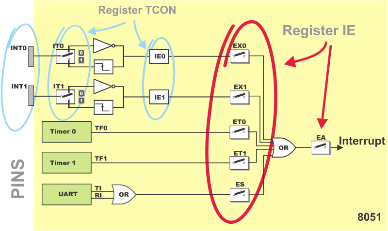
Interrupt Process
- Trigger: An interrupt source (external pin, timer overflow, etc.) is triggered.
- Completion of Current Instruction: The 8051 completes executing its current instruction.
- Saving State: The microcontroller automatically pushes the current Program Counter (PC) onto the stack.
- Jump to ISR: The 8051 jumps to the pre-determined memory address of the corresponding Interrupt Service Routine (ISR).
- ISR Execution: The ISR code executes, handling the event that triggered the interrupt.
- Returning: After the ISR completes, a 'RETI' instruction pops the PC value from the stack, resuming the original program flow.
Interrupt Control Registers
- IE (Interrupt Enable): Enables or disables specific interrupts globally and individually within the system.
- IP (Interrupt Priority): Assigns priority levels to each interrupt source. If multiple interrupts occur simultaneously, the one with higher priority is serviced first.
Interrupt Vector Table
| Interrupt | Flag | Interrupt Vector Address |
|---|---|---|
| Reset | - | 0000H |
| INT0 | IE0 | 0003H |
| Timer 0 | TF0 | 000BH |
| INT1 | IE1 | 0013H |
| Timer 1 | TF1 | 001BH |
| Serial | TI/RI | 0023H |
Table: Interrupt Vector Table
Key Points
- Priority: The 8051 has a fixed interrupt priority structure (e.g., INT0 has the highest priority).
- Masking: Interrupts can be turned on or off selectively using the IE register.
- Nesting: Interrupts can potentially interrupt other interrupts, depending on their priority.
- Enabling Interrupts: Interrupts must be enabled individually (e.g., IE0, ET0) and globally (EA = 1 in the IE register).
- Interrupt Service Routines (ISRs): ISRs contain the code to handle specific interrupt events. The microcontroller automatically jumps to the corresponding ISR's address in the vector table when an enabled interrupt occurs.
IE Register
What is the IE Register?
- The IE (Interrupt Enable) register is an 8-bit, bit-addressable Special Function Register (SFR) within 8051 microcontrollers.
- Each bit in this register controls the enabling or disabling of specific interrupts within the system.
IE Register Structure (Address: 0A8H, Byte addressable):
| IE.7 | IE.6 | IE.5 | IE.4 | IE.3 | IE.2 | IE.1 | IE.0 |
|---|---|---|---|---|---|---|---|
| EA | - | - | ES | ET1 | EX1 | ET0 | EX0 |
Table: IE Register Structure
Here's the breakdown of the IE Register's bit functionality:
-
EA (Enable All):
- '1' = Enables all interrupt sources (if their individual bits are also set to '1').
- '0' = Disables all interrupts, regardless of other bit settings.
-
Unused (3 bits): These bits are typically reserved and have no assigned functionality.
-
ES (Enable Serial Interrupt):
- '1' = Enables serial port interrupt.
- '0' = Disables serial port interrupt.
-
ET1 (Enable Timer 1 Interrupt):
- '1' = Enables the interrupt generated by Timer 1 overflow.
- '0' = Disables the Timer 1 interrupt.
-
EX1 (Enable External Interrupt 1):
- '1' = Enables the external interrupt 1.
- '0' = Disables the external interrupt 1.
-
ET0 (Enable Timer 0 Interrupt):
- '1' = Enables the interrupt generated by Timer 0 overflow.
- '0' = Disables the Timer 0 interrupt.
-
EX0 (Enable External Interrupt 0):
- '1' = Enables the external interrupt 0.
- '0' = Disables the external interrupt 0.
| Bit | Function |
|---|---|
| EA | Global interrupt enable/disable Bit |
| ES | Enable Serial Interrupt Bit |
| ET1 | Enable Timer1 Interrupt Bit |
| EX1 | Enable External Interrupt 1 Bit |
| ET0 | Enable Timer0 Interrupt Bit |
| EX0 | Enable External Interrupt 1 Bit |
Table: IE Register Function
How Interrupts Work with IE
- Global Enable: The EA bit in the IE register must be set to '1' for any interrupt to function.
- Individual Enable: Even if EA is set to '1', a specific interrupt request will be recognized only if the corresponding bit in the IE register is also set to '1'.
Examples
-
Enabling All Interrupts
IE = 0xFF; // Set all bits in IE to '1' -
Enabling Only Timer 0 and External Interrupt 1
IE = 0x89; // Sets the ET0 and EX1 bits, the rest are '0'
Important Note:
- Interrupts must also be configured in other registers for them to be active. For example:
- Timer interrupts require the timers to be started (TRx = '1' in TCON).
- External interrupts may need edge or level triggering configured (ITx bits in TCON).
- The 8051 has a priority system for multiple simultaneous interrupts. You can control the priority using the IP (Interrupt Priority) register.
IP Register
What is the IP Register?
- The IP (Interrupt Priority) register is an 8-bit, bit-addressable Special Function Register (SFR) used to manage the priority of interrupt sources in 8051 microcontrollers.
- When multiple interrupts occur simultaneously, the IP register helps the system determine which interrupt to handle first.
IP Register Structure (Address: 0B8H, Byte addressable)
| IP.7 | IP.6 | IP.5 | IP.4 | IP.3 | IP.2 | IP.1 | IP.0 |
|---|---|---|---|---|---|---|---|
| - | - | - | PS | PT1 | PX1 | PT0 | PX0 |
Table: IP Register Structure
Each bit in the IP register is assigned a specific interrupt source, providing two levels of priority (high or low):
-
Unused (3 bits): These bits are typically reserved and have no assigned functionality.
-
PS (Serial Interrupt Priority):
- '1' = High priority.
- '0' = Low priority.
-
PT1 (Timer 1 Interrupt Priority):
- '1' = High priority.
- '0' = Low priority.
-
PX1 (External Interrupt 1 Priority):
- '1' = High priority.
- '0' = Low priority.
-
PT0 (Timer 0 Interrupt Priority):
- '1' = High priority.
- '0' = Low priority.
-
PX0 (External Interrupt 0 Priority):
- '1' = High priority.
- '0' = Low priority.
| Bit | Function |
|---|---|
| PS | Serial Interrupt Priority Bit |
| PT1 | Timer1 Interrupt Priority Bit |
| PX1 | External Interrupt 1 Priority Bit |
| PT0 | Timer0 Interrupt Priority Bit |
| PX0 | External Interrupt 0 Priority Bit |
Table: IP Register Function
Default Interrupt Priority
| Priority | Interrupt source | Intr. bit / flag |
|---|---|---|
| 1 | External Interrupt 0 | INT0 |
| 2 | Timer Interrupt 0 | TF0 |
| 3 | External Interrupt 1 | INT1 |
| 4 | Timer Interrupt 1 | TF1 |
| 5 | Serial interrupt | (TI/RI) |
Table: Default Interrupt Priority
How Interrupt Priorities Work with IP
-
Interrupt Occurrence: When one or more interrupts occur, the 8051 checks the corresponding bits in the IP register.
-
Priority Handling
- Higher priority interrupts always take precedence over lower priority interrupts.
- If multiple interrupts of the same priority level occur, then the 8051 uses a predefined internal polling sequence to determine the order for servicing the interrupts.
Examples
-
Configuring Timer 0 as Highest Priority, External Interrupt 1 as Lowest
IP = 0x12; // Sets PT0 to '1' (high), PX1 to '0' (low), others remain '0' -
Setting All Interrupts to Low Priority
IP = 0x00; // All bits set to '0' for low priority
Important Notes:
-
The IP register only determines the priority among simultaneously occurring interrupts. The interrupt itself still needs to be enabled globally (EA bit in the IE register) and individually (Ex and ETx bits in the IE register).
-
The priority structure and internal polling sequence for the 8051 microcontroller can be found in your specific microcontroller's datasheet.