Unit 5: Interfacing & Applications of Microcontroller
Guide to interfacing various devices with 8051 microcontroller
Interfacing Input Devices or Sensors
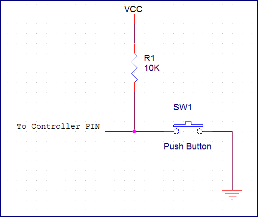
Push Button Switches
Hardware Setup
-
Connect the Pushbutton: One pin of the pushbutton is connected to an input port pin on the 8051 (let's say P1.0). The other pin is connected to ground (GND).
-
Pull-up Resistor: Connect a pull-up resistor (10K ohms is typical) between the pushbutton's input pin and VCC (power supply). This ensures the input pin reads a definite HIGH when the button is not pressed.
Logic
- Pressed: When pressed, the button connects the input pin to GND, reading a logic LOW (0).
- Released: When released, the pull-up resistor pulls the input pin HIGH (1).
Assembly Code
Assembly
Explanation (Assembly):
- JB: "Jump if Bit" checks the specified bit (P1.0).
- MAIN_LOOP: Continuously polls the button state.
- BUTTON_PRESSED: This section executes if the button is pressed.
C Code
C
Explanation (C):
- sbit: Defines a single bit variable for easy access.
- while(1): Creates an infinite loop.
- if/else: Checks the button state and executes appropriate code blocks.
Remember:
- Replace placeholders: Change '...' in the code blocks with the actual actions you want to perform when the button is pressed or not pressed (like turning an LED on/off, etc.).
- Debouncing: In real-world scenarios, you'll likely need to add debouncing code (software or a small delay circuit) to prevent false readings due to mechanical bouncing of the button contacts.
DIP Switch
Hardware Setup
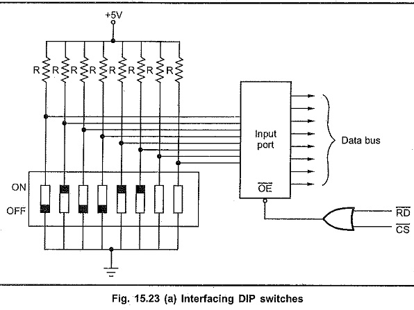
- Connect the DIP Switch: Connect one side of each switch in the DIP package to separate input pins on the 8051 microcontroller (for example, P1.0 through P1.7 for 8 switches).
- Pull-up/Pull-down Resistors: Depending on your DIP switch configuration, you'll need one of the following:
- Pull-up resistors: If your DIP switches connect to ground when ON, connect pull-up resistors (around 10K ohms) between each switch pin and VCC.
- Pull-down resistors: If your DIP switches connect to VCC when ON, connect pull-down resistors between each switch pin and ground.
Logic
- Switch ON: Provides a definite HIGH (1) or a definite LOW (0) to the input pin, depending on your resistor configuration.
- Switch OFF: The resistor pulls the input pin to the opposite state.
Assembly Code
Assembly
Explanation (Assembly):
- MOV A, P1: Reads the state of all DIP switch pins connected to Port 1.
- Individual bits in the Accumulator (A) now represent the switch positions. You'll need logic to isolate and handle these bits according to your desired functionality.
C Code
C
Explanation (C):
- DIP_value: This variable holds the current state of the DIP switches.
- P1: Reading the port directly gives you the switch states.
- Individual bits of
DIP_valuerepresent switches. Write logic to handle them according to your needs.
Important Points
- Adapting the Code: Modify the bit handling logic in the code examples to match the desired functionality based on your DIP switch arrangement.
- Masking (Assembly): Use bitwise operations (AND, OR) to isolate specific bits if needed.
- Bit-shifting (C): Use bit shifts (
>>or<<) to check or manipulate individual switch states.
Example: Turn on LED connected to P2.0 if DIP switch 1 is ON
Assembly:
Assembly
C:
C
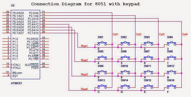
Keypad Interfacing
Hardware Setup
-
Keypad Connections:
- Columns: Connect the four column wires of the keypad to pins P2.0 - P2.3.
- Rows: Connect the four row wires of the keypad to pins P2.4 - P2.7.
-
Pull-up Resistors: Add pull-up resistors (around 10K ohms) between each column pin (P2.0-P2.3) and VCC. These ensure definite HIGH signals on the columns when no key is pressed.
Key Scanning Logic
-
Initialize: Configure the column pins (P2.0-P2.3) as outputs and the row pins (P2.4-P2.7) as inputs.
-
Column Drive: Sequentially drive one column LOW at a time, keeping the others HIGH.
-
Row Read: Read the state of the row pins. If any row pin is LOW, it indicates a keypress at the intersection of the active column and the detected row.
-
Debouncing: Implement a short delay or debouncing algorithm to avoid false readings due to keypress bounce.
Assembly Code
Assembly
Replace COLUMN_PATTERN with values like 0x0E, 0x0D, 0x0B, 0x07 to activate one column at a time.
C Code
C
Important Notes
- Key Mapping: Create a lookup table to map row/column combinations to their corresponding key values.
- Debouncing: Implement a delay-based or interrupt-based debouncing mechanism.
- Code Completion: The provided snippets demonstrate scanning. You'll need to add logic to determine the pressed key based on the detected row/column and implement debouncing.
Potentiometer Interfacing
Hardware Setup
-
Connecting the Potentiometer:
- Middle Pin: Connect the center (wiper) pin of the potentiometer to one of the 8051's analog input channels (ADC0804/0808).
- Outer Pins: Connect one outer pin to VCC (+5V) and the other to ground (GND).
-
Connect ADC (ADC0804/0808):
- ADC Pins: Connect its analog input to the potentiometer's wiper pin.
- Digital Pins: Interface it with the 8051 for data transfer, clocking, and control signals.
How it Works
- Variable Voltage Divider: The potentiometer acts as a variable voltage divider. As you rotate its knob, the output voltage on the center pin changes between 0V and 5V.
- ADC Conversion: The ADC (Analog to Digital Converter) converts this analog voltage into a digital value that the 8051 can understand.
Assembly Code (ADC0804/0808)
Assembly
C Code (ADC0804/0808)
C
Important Considerations
-
ADC ReSolution:**** The digital value from the ADC (0-1023 for 10-bit resolution) represents the position of the potentiometer's wiper. You might need to scale or map this value to a meaningful range within your application.
-
ADC Control: Refer to your ADC0804/0808 datasheet for specific instructions and registers to set up the ADC correctly.
Examples of Usage
- Brightness control: Adjust the brightness of an LED.
- Speed Control: Control the speed of a motor.
- Menu Navigation: Use it as an analog input for menu selection.
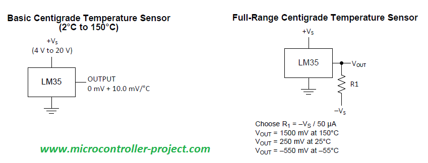
LM35 Temperature Sensor
LM35 Basics
- Analog temperature sensor
- Output voltage is directly proportional to temperature in degrees Celsius (10mV/°C)
- Example: 250mV output = 25°C
Hardware Setup
-
Connect the LM35:
- VCC: Connect to the 8051's power supply (+5V)
- Output: Connect the LM35's output pin to an analog input channel on the ADC0804/0808 ADC chip.
- GND: Connect to a common ground.
-
Connect the ADC0804/0808:
- ADC Pins: Connect its analog input to the LM35 output.
- Digital Pins: Interface the ADC's data, clock, and control pins with the 8051 microcontroller.
ADC Logic
- Initialization: Configure the ADC (resolution, conversion mode, etc.).
- Start Conversion: Send a command to the ADC to initiate a conversion of the LM35's analog voltage.
- Read Digital Result: Once the conversion is complete, read the digital output from the ADC. This digital value represents the temperature.
- Conversion to Degrees Celsius: Scale the digital value based on the ADC's resolution and the LM35's output characteristics (10mV/°C).
Assembly Code (ADC0804/0808)
Assembly
C Code (ADC0804/0808)
C
Notes:
- ADC Driver: You'll likely need specific instructions on controlling the ADC0804/0808, which will depend on how it's interfaced with the 8051.
- Calculation: In the C code, the calculation assumes a 10-bit ADC and a 5V reference voltage.
- Code is Simplified: This omits error handling and some setup details.
Interfacing Output Devices or Actuators
LEDs
Hardware Setup
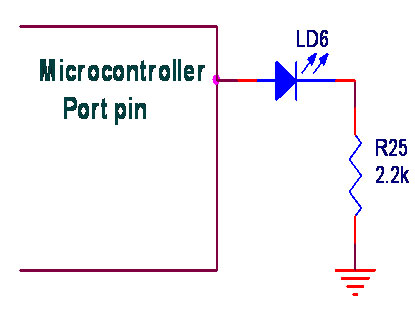
- Connect LED: Connect the longer leg (anode) of the LED to an I/O pin of the 8051 (let's say P1.0) through a current-limiting resistor (around 220 ohms). Connect the shorter leg (cathode) to ground (GND).
Logic
- ON: Drive the I/O pin HIGH (1) to turn the LED on.
- OFF: Drive the I/O pin LOW (0) to turn the LED off.
Assembly Code (Blinking LED)
Assembly
Explanation (Assembly)
- MOV P1, #00H: Initializes port P1 as output.
- SETB/CLR: Controls the LED (ON/OFF)
- CALL DELAY: Creates a delay between LED state changes.
- DELAY subroutine: Provides a simple adjustable delay.
C Code (Blinking LED)
C
Explanation (C)
- sbit LED: Conveniently defines an alias for the LED pin.
- delay function: Creates a software delay.
- LED = 1/0: Turns the LED on and off.
Key Points:
- Resistor: Always use a current-limiting resistor with LEDs to prevent damage.
- Delay: Adjust delay values to control blink speed.
- I/O Configuration: Ensure the pin connected to the LED is configured as output.
Blink 8 LEDs
Hardware Setup
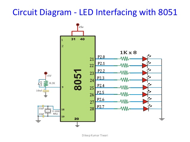
- 8 LEDs: Choose standard LEDs considering the current requirements of the 8051's I/O ports.
- Current-Limiting Resistors: Calculate the appropriate resistor values for your specific LEDs to prevent damage (search for an online "LED resistor calculator" if needed).
- 8051 Microcontroller: We'll assume you have an 8051 development board with an I/O port (e.g., Port 1).
- Connections:
- Connect one leg of each LED to a separate pin on Port 1 of the 8051 (P1.0 to P1.7).
- Connect the other leg of each LED through a current-limiting resistor to ground.
Programming (Assembly)
Here's a simple 8051 assembly program to repeatedly turn the LEDs on and then off with a delay:
Assembly
Explanation
-
MAIN_LOOP:
MOV A, #FFH: Loads the accumulator with FFH (all bits 1), which will turn all LEDs on.MOV P1, A: Sends this value to Port 1.CALL DELAY: Calls a subroutine to create a delay.MOV A, #00H: Loads the accumulator with 00H (all bits 0), which will turn all LEDs off.SJMP MAIN_LOOP: Creates an infinite loop.
-
DELAY Subroutine:
- Provides a simple software delay using nested loops. You might want a more precise timer-based delay in a real application.
Key Points:
- Port Choice: I used Port 1(P1); adapt the code if you connect the LEDs to a different port.
- LED Polarity: If your LEDs light up in the opposite manner, reverse the logic (use 00H to turn them on and FFH to turn them off)
- Delay Adjustment: Modify the values in the DELAY subroutine to change the on and off duration.
LED Fading using PWM
Understanding PWM
- PWM stands for Pulse Width Modulation.
- It involves rapidly turning a digital pin ON and OFF at varying ratios.
- The longer the ON time relative to the OFF time (the duty cycle), the brighter the LED appears.
- Our eyes perceive the rapid blinking as different levels of brightness.
Methods for PWM on the 8051
-
Software PWM:
- Control PWM entirely in your code using delays and pin manipulation.
- Pros: Flexible, doesn't require specific hardware.
- Cons: Can consume CPU cycles, limiting the complexity of other code running simultaneously.
-
Hardware PWM (Timer Generated):
- Many 8051 variants have built-in timers that can generate PWM signals.
- Pros: Efficient, frees up your CPU for other tasks.
- Cons: Less flexible, depends on the available timers and their features.
Implementing Software PWM
Assembly Code
Assembly
C Code
C
7-Segment Displays
Assumptions
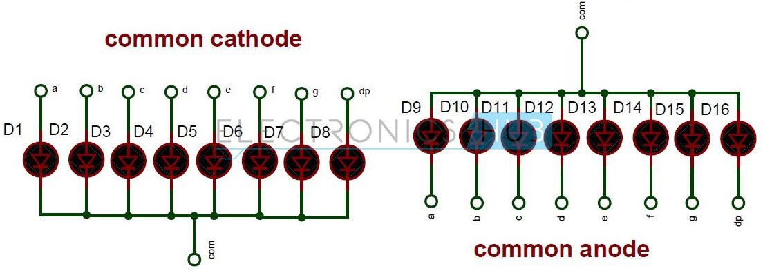
- Common Anode Display: The segments have a common positive connection. We'll control them by sinking current (connecting to ground) through the 8051's pins.
- Adapt the segment patterns if you have a Common Cathode display.
- Single Digit: We'll interface a single digit display. This can be extended for multiple digits using multiplexing techniques.
- Connections: We'll assume you'll connect the 7-segment pins (a through g) to a port of the 8051 (e.g., Port 1).
Hardware Setup
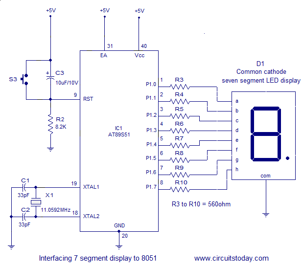
- 7-Segment Display: Choose a common anode 7-segment LED display.
- Current-Limiting Resistors: Calculate and use resistors in series with each segment LED to prevent damage. Search for a "LED resistor calculator" to find the right values.
- Connections:
- Connect the anodes of all segments (a through g) to the corresponding pins of Port 1 (P1.0 through P1.6) of the 8051.
- Connect the common anode pin to the power supply (+5V).
- Connect each segment's cathode through the resistor to ground.
Lookup Table
Create a lookup table in your program memory that maps the digit you want to display (0-9) to the corresponding segment patterns:
Assembly
Note: For a common anode display, '1' means the segment should be ON, so it's connected to ground.
Assembly Code Example
Assembly
Explanation
- Table Usage: The code loads the digit to be displayed into R0, uses indirect addressing to get the corresponding pattern from the lookup table, and sends it to the display port.
- Multiplexing: If you have multiple 7-segment displays, you need to switch between them rapidly and update the display port accordingly to create the illusion they are all on simultaneously.
Important:
- Port Output: Ensure the port you use is configured as output.
- Resistors: Don't forget the current-limiting resistors!
LCD Interfacing
Hardware Setup
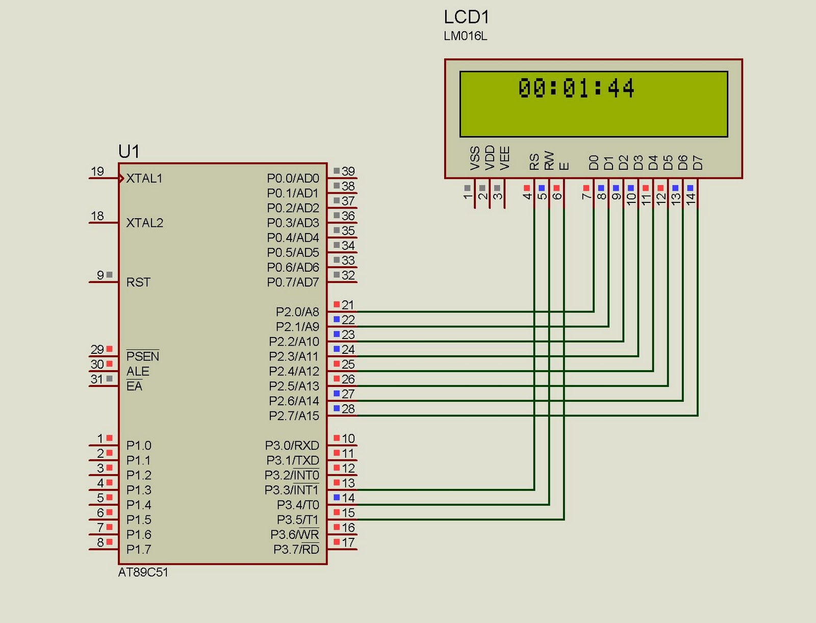
- LCD: We'll assume a standard 16x2 character LCD module with a common HD44780 compatible controller.
- Connections:
- Data Pins (D0-D7): Connect to an 8051 I/O Port (e.g., Port 2)
- Control Pins:
- RS (Register Select): Connect to an 8051 pin (e.g., P1.0)
- RW (Read/Write): Connect to an 8051 pin (e.g., P1.1)
- E (Enable): Connect to an 8051 pin (e.g., P1.2)
- Contrast Adjustment (Vo): Connect to a potentiometer for controlling display contrast.
- Backlight (if present): Power according to its requirements.
Assembly Programming
Here's an 8051 assembly program to initialize the LCD and display "Welcome":
Assembly
Explanation
- Constants:
LCD_PORTis defined to make the code adaptable if your connections change. - Subroutines: These encapsulate the interaction details with the LCD (sending commands, sending data), making the main program cleaner. You'll need to fill in the details of these subroutines according to your LCD's datasheet.
- Main Program:
- Calls
LCD_INITto configure the LCD. - Sends commands to select the desired display mode (2 lines, 5x7 font) and clear the display.
- Sends each character of the message "Welcome" to the LCD using
LCD_DATA.
- Calls
Key Points
- LCD Datasheet: You MUST adapt the initialization and command sequences based on your specific LCD module.
- 8051 Timing: You might need short delays within the subroutines to ensure the LCD processes commands correctly.
- Subroutine Implementation: The core logic of sending commands/data to the LCD involves setting the RS/RW lines, placing data on the data port, and pulsing the Enable pin.
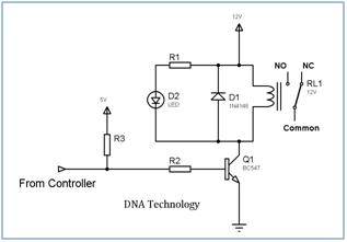
Relays
Relays Explained
- Electromagnetic Switches: Relays are electromechanical switches that use an electromagnet to control the opening and closing of contacts.
- Coil and Contacts: They consist of a coil, an armature (lever), and a set of contacts.
- Activation: When current flows through the coil, it generates a magnetic field that attracts the armature, causing the contacts to switch states (open or closed).
Interfacing with 8051
-
Driver Circuit: The 8051 microcontroller cannot directly provide the high current needed to operate the relay coil. Therefore, a driver circuit is necessary.
- Transistor: A common approach is to use a transistor as a switch, controlled by the 8051 output pin.
- Driver ICs: Dedicated driver ICs like the ULN2003 are also commonly used for easier interfacing with multiple relays.
-
Connections:
- Connect the control pin of the transistor (or driver IC) to an output pin of the 8051.
- Connect the relay coil to the collector and emitter of the transistor (or the corresponding pins on the driver IC).
- Connect the relay's common contact to your desired circuit, and the normally open (NO) or normally closed (NC) contact based on your switching needs.
Assembly Code Example
Assembly
C Code Example
C
Explanation of the Code:
- Relay Control State: We define a variable (
R0in assembly,RELAY_CTRLin C) to represent the relay state (on/off). - Main Loop: The code continuously loops, turning the relay on and off with adjustable delays using a simple delay routine.
- Assembly: The
SETBinstruction is used to directly set the P1.0 pin high. - C: The
sbitdirective is used to define a bit-level controllable variable for the relay control pin.
DC Motors
L293D IC
It is a versatile integrated circuit that can be used to drive various types of DC motors and steppers motors.
Key Features:
- Dual H-bridge driver: It can control two DC motors or one bipolar stepper motor simultaneously in both directions (forward and reverse) by reversing the polarity of the voltage applied to the motor.
- Wide operating voltage: It can operate with a voltage range of 4.5V to 36V, making it suitable for various applications.
- High current capability: Each channel can deliver a continuous current of up to 600mA, making it suitable for driving small to medium-sized DC motors.
- Logic level inputs: The control inputs are compatible with digital logic levels (0V to 5V), allowing for easy control with microcontrollers like the 8051.
Pin Configuration:
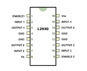
- Inputs (2 per channel):
- IN1 and IN2: Control the direction of the connected motor (forward/reverse).
- Outputs (2 per channel):
- OUT1 and OUT2: Connect to the motor terminals.
- Power supply:
- Vcc: Positive power supply (4.5V to 36V).
- GND: Ground.
- Enable pins (optional):
- Enable1 and Enable2: Enable or disable the respective motor driver channel.
Applications:
- Robot locomotion (driving wheels)
- Controlling conveyor belts
- Operating solenoid valves
- Remote-controlled toys and cars
How it Works:
By applying specific high or low logic signals to the IN1 and IN2 pins, you can control the direction and rotation of the connected DC motor. The L293D internally manages the power flow to the motor terminals (OUT1 and OUT2) based on the input signals.
DC Motor Interfacing with 8051
Hardware Connections:
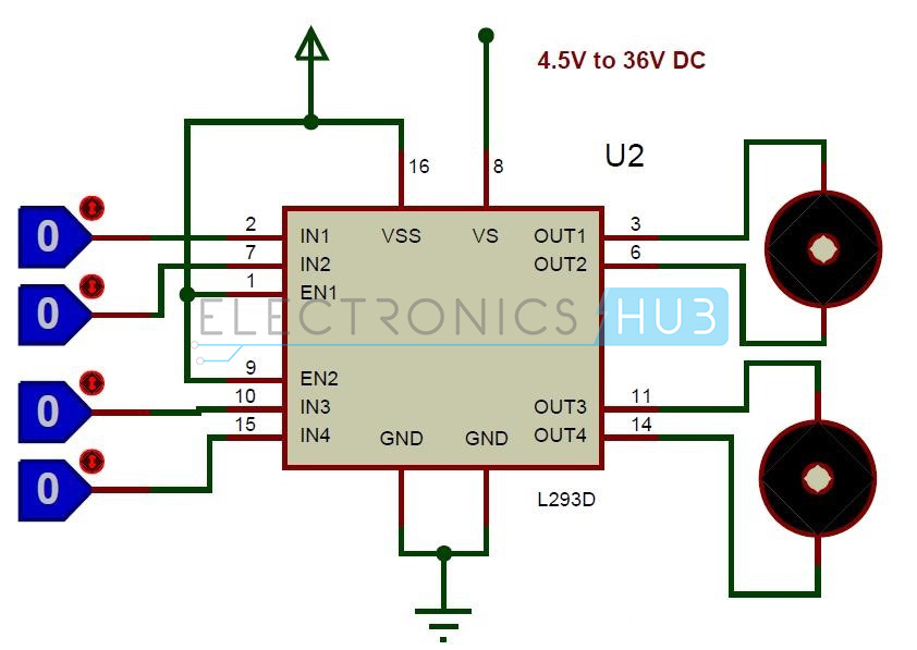
-
Connect the L293D motor driver:
- Vcc of the L293D to +5V power supply.
- GND to ground.
- Connect IN1, IN2, IN3, and IN4 of the L293D to four control pins (e.g., P1.0 to P1.3) of the 8051.
- Connect the motor to the OUT1 and OUT2 pins of the L293D's first channel (Channel 1).
-
Connect the motor supply:
- Connect the positive terminal of the motor to a separate power supply (voltage appropriate for your motor, typically 6V to 12V).
- Connect the negative terminal of the motor to the ground.
Assembly Code:
Assembly
C Code:
C
Explanation:
- Motor Control States:
- We define two variables (
R0andR1) in assembly orsbitdefinitions in C to represent the forward and reverse motor control states.
- We define two variables (
- Main Loop:
- The code continuously runs in a loop, setting the motor direction pin values (P1.0 and P1.1) based on the defined states (
R0orR1).
- The code continuously runs in a loop, setting the motor direction pin values (P1.0 and P1.1) based on the defined states (
- Delay:
- A simple delay loop is included to control the duration of each direction (forward and reverse).
- Adjust the delay value (
#100in assembly,100in C) to change the motor speed.
Stepper Motors
Basics of Stepper Motors
- Type of Motor: Stepper motors are brushless DC motors that convert electrical pulses into precise, discrete rotational movements.
- Steps: Their unique feature is that the shafts rotate in fixed angular increments (steps) rather than continuously. This allows for highly accurate positioning without feedback sensors (open-loop control).
- Stator and Rotor:
- Stator: Stationary part holding multiple electromagnetic coils.
- Rotor: Typically a permanent magnet that rotates in response to energized stator coils.
Types of Stepper Motors
-
Unipolar Stepper Motors
- Most Common
- Each coil has a center tap.
- 5, 6, or 8 wire configurations possible.
-
Bipolar Stepper Motors
- No center taps on coils.
- Require reversing coil currents to change direction.
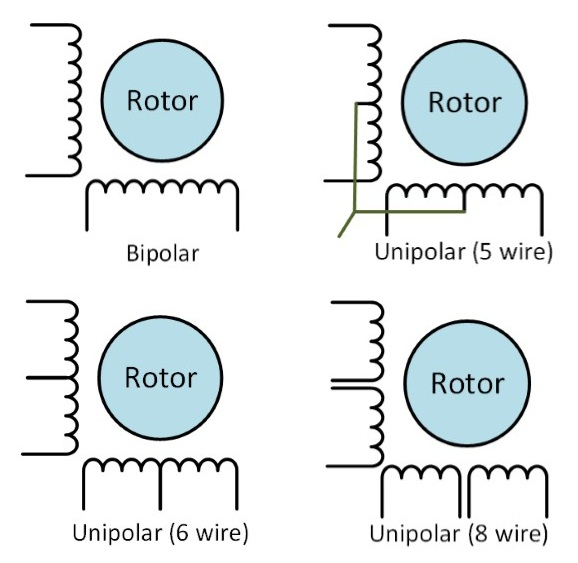
Wiring Arrangements
- Unipolar (5-wire): Only half of each coil is used at a time.
- Unipolar (6-wire): Full coil use is possible for increased torque.
- Unipolar (8-wire): Provides the greatest wiring flexibility (unipolar or bipolar operation).
- Bipolar (4-wire): The coil current direction needs to be reversed for rotation direction control. This requires an H-bridge driver circuit.
Stepper Motor Drive Modes
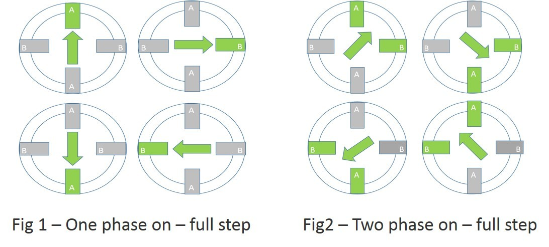
- Wave Drive (One-Phase On)
- Simpliest to control.
- Only one coil is energized at a time.
- Lower torque and holding strength.
| A | B | C | D |
|---|---|---|---|
| 1 | 0 | 0 | 0 |
| 0 | 1 | 0 | 0 |
| 0 | 1 | 0 | 0 |
| 0 | 0 | 0 | 1 |
Table: Wave Drive (One-Phase On)
- Full-Step Drive (Two-Phase On)
- Two coils are energized simultaneously.
- Provides increased torque compared to wave drive.
| A | B | C | D |
|---|---|---|---|
| 1 | 1 | 0 | 0 |
| 0 | 1 | 1 | 0 |
| 0 | 0 | 1 | 1 |
| 1 | 0 | 0 | 1 |
Table: Full-Step Drive (Two-Phase On)
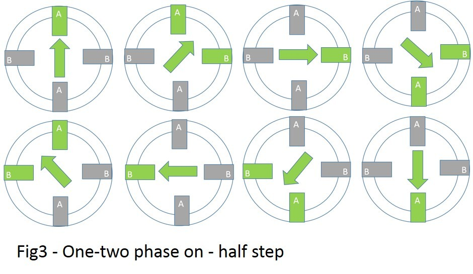
- Half-Step Drive
- Alternates between wave drive and full-step drive.
- Doubles the effective resolution of the motor (smaller step angles).
- Maintains good torque levels.
| A | B | C | D |
|---|---|---|---|
| 1 | 0 | 0 | 0 |
| 1 | 1 | 0 | 0 |
| 0 | 1 | 0 | 0 |
| 0 | 1 | 1 | 0 |
| 0 | 0 | 1 | 0 |
| 0 | 0 | 1 | 1 |
| 0 | 0 | 0 | 1 |
| 1 | 0 | 0 | 1 |
Table: Half-Step Drive
Interfacing with the 8051
-
GPIO Pins: Connect output pins from the 8051 to a compatible stepper motor driver.
-
Stepper Motor Driver:
- ULN2003: Simple and suitable for unipolar stepper motors.
- H-bridge Drivers (e.g., L293D, A4988, etc.): For bipolar motors, as they can reverse current flow.
-
Step Sequencing: The 8051 generates the correct pulse sequence (wave, full, or half-step) to control the stepping pattern and direction of the motor.
Stepper Motor Interfacing with 8051
Hardware Connections:
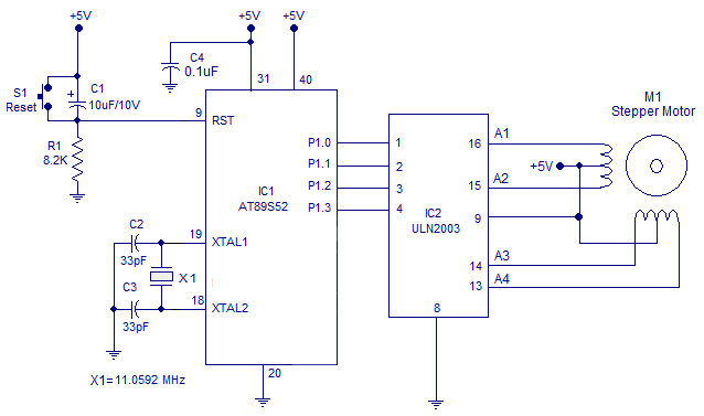
Here's a breakdown of the connections:
- Microcontroller (8051):
- Port 1 (P1) is connected to the input pins of the ULN2003 (A1, A2, A3, and A4).
- ULN2003 Driver:
- Input pins (A1-A4) are connected to the microcontroller (P1.0-P1.3).
- Output pins (B1-B4) are connected to the stepper motor coils in the correct sequence according to the motor's wiring diagram.
- Stepper Motor:
- The four coils of the stepper motor are connected to the corresponding output pins (B1-B4) of the ULN2003 driver.
- Power Supply:
- The microcontroller and ULN2003 share a common 5V power supply.
ULN2003 (Function of ULN2003)
The ULN2003 is a Darlington transistor array, which essentially acts as an amplifier. It allows the low-current outputs of the microcontroller to drive the higher current required by the stepper motor coils.
Stepper Motor Driving Principle
By applying specific pulse sequences to the stepper motor coils in a particular order, the motor shaft rotates in steps. Different pulse sequences can be used to achieve different rotation directions and stepping patterns.
Assembly Code Example
Assembly
C Code Example
C
Explanation of the Code:
- The code defines a step pattern which is a sequence of values representing the energized coils at each step.
- A loop continuously outputs the step pattern to the ULN2003, causing the motor to rotate one step at a time.
- The delay loop controls the speed of the motor's steps.
- The assembly code uses bit manipulation (
RLC) to rotate the step pattern for the next step. - The C code uses an array to store the step pattern and an index to keep track of the current step.
ADC (Analog-to-Digital Converter)
-
Purpose: ADCs are electronic circuits that convert continuous analog voltage signals into discrete digital representations. This is essential for microcontrollers, which primarily work with digital data.
-
Process:
- Sampling: The ADC takes "snapshots" of the analog input signal at regular intervals.
- Quantization: Each sample's voltage level is compared to a reference voltage and mapped to a discrete digital value.
- Output: The result is a binary code representing the closest digital approximation of the analog input.
-
Key Characteristics
- ReSolution:**** Number of bits in the output code (e.g., 8-bit, 10-bit). Higher resolution means finer digital representations of the analog signal.
- Sampling rate: How frequently the ADC samples the analog input (measured in samples per second).
- Accuracy: How closely the digital output reflects the true analog input.
ADC0804 Overview
- Type: Successive approximation ADC (SAR ADC).
- Features:
- 8-bit resolution (256 discrete output levels)
- Single analog input channel
- Requires an external clock signal to control conversion time
- TTL compatible for easy interfacing with microcontrollers
- Low power consumption
- Relatively simple and inexpensive
Pinout (20-pin DIP package)
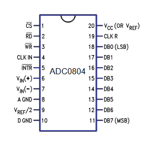
- Analog Input:
- VIN(+) : Positive analog input
- VIN(-): Negative analog input (often connected to ground for single-ended operation)
- Reference Voltage:
- Vref/2: Reference voltage input (sets the range for conversion)
- Control Signals:
- CS: Chip Select (active low)
- RD: Read (active low)
- WR: Write (active low)
- INTR: Interrupt (active low, signals end of conversion)
- CLK IN: External clock input
- Digital Outputs:
- D0 - D7: 8-bit digital output
Typical Usage Scenario
- Connect Signals Interface the ADC0804 with a microcontroller, providing necessary control signals and reading the digital output.
- Apply Reference Voltage: Set the reference voltage (Vref/2) to determine the input voltage range you want to measure.
- Initiate Conversion: Use the control signals (CS, RD, WR) to start an analog to digital conversion.
- Clocking: Provide an external clock signal (if no internal clock is used) to drive the conversion process.
- Read Result: When the conversion completes, signaled by the INTR pin or by polling, read the 8-bit digital output.
ADC0804 Interfacing
Assumptions
- ADC0804 Connections:
- Analog Input (VIN+) to the signal you want to measure.
- VIN- to ground.
- Control Pins (CS, RD, WR, INTR) to 8051 I/O pins.
- Data Pins (D0-D7) to an 8051 port.
- 8051 Hardware: We'll use Port 1 (P1) for the ADC data and sample control signals on the 8051.
Hardware Setup
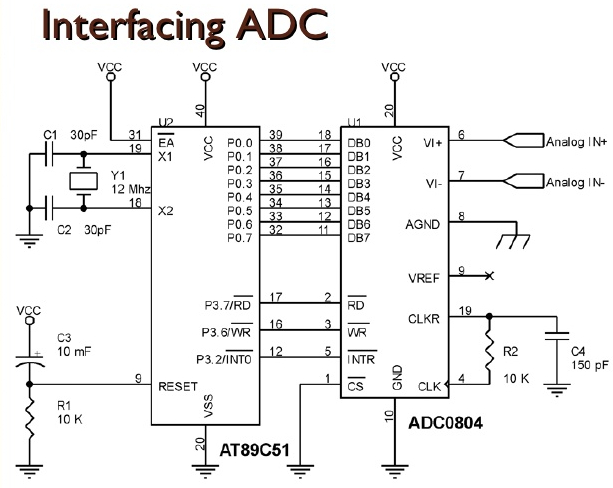
- Connect ADC0804 and 8051: Interface the ADC pins to your 8051 microcontroller as described above.
- Reference Voltage: Apply an appropriate reference voltage to the ADC's Vref/2 pin. This determines the full-scale input range.
- Clock Source: If your ADC0804 doesn't have an internal clock, connect an external clock signal to the CLK IN pin.
Assembly Code
Assembly
C Code
C
Important Notes
- Control Pins: Adjust the pin assignments in the code if you're using different 8051 pins.
- Error Handling: Implement error checks in production code.
- Timing: Consider the ADC0804's conversion time and adjust delays or polling accordingly.
- Calculation: Scale the raw ADC value to a meaningful voltage based on your reference voltage.
DAC (Digital-to-Analog Converter)
-
Purpose: DACs are electronic circuits that do the opposite of ADCs – they convert digital codes into corresponding analog voltage levels. This allows microcontrollers to generate smooth analog signals for various applications.
-
Process:
- Digital Input: The DAC accepts a binary code as input.
- Reference Voltage: A stable reference voltage determines the full-scale output range of the DAC.
- Conversion: The DAC generates an analog voltage proportional to the digital input code and the reference voltage.
-
Key Characteristics:
- ReSolution:**** The number of bits in the input code (e.g., 8-bit, 10-bit). Higher resolution means more fine-grained analog output levels.
- Accuracy: How closely the analog output represents the target value based on the digital input.
- Settling Time: How quickly the DAC's output stabilizes to a new voltage after a change in the digital input.
DAC0808 Overview
- Type: A common R-2R ladder type DAC.
- Features:
- 8-bit resolution (256 discrete output levels)
- Single analog output
- Reference current input to set output range
- Can be used in multiplying mode for greater precision
- TTL compatible for easy interfacing with microcontrollers
- Fast settling time
Pinout (16-pin DIP package)
- Digital Inputs:
- I0 - I7: Least significant bit (LSB) to most significant bit (MSB)
- Reference Current
- Iref: Determines the output current (and thus the output voltage range)
- Analog Output
- IOUT: The analog output current
- Other
- Vcc: +5V Power supply
- GND: Ground
Typical Usage Scenario
- Connect Signals: Interface the DAC0808 with a microcontroller to send digital data.
- Set Reference Current: Apply the required reference current to Iref. This will determine the maximum output voltage and the step size per digital input change.
- Send Digital Code: Write the 8-bit digital code to the DAC's input pins.
- Output: The DAC outputs a corresponding analog current at IOUT. Often, this current is converted to an analog voltage by using an external op-amp circuit.
DAC0808 Interfacing
Assumptions
-
DAC0808 Connections:
- Digital inputs (I0-I7) connected to an 8051 port.
- Iref connected to a suitable current source to set the output range.
- External op-amp circuit (if needed) to convert the DAC output current (IOUT) into a usable voltage.
-
8051 Hardware: We'll use Port 1 (P1) for sending data to the DAC0808.
Hardware Setup
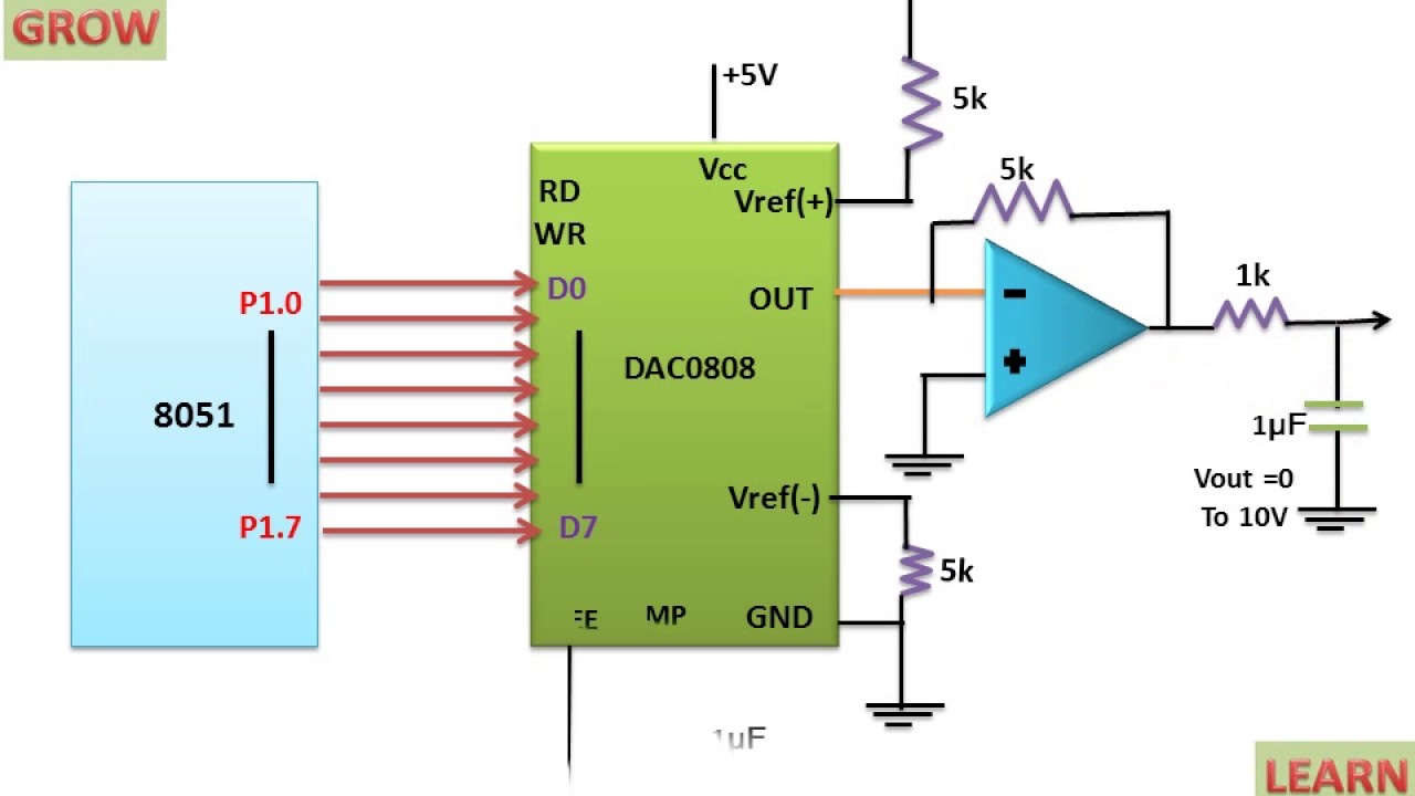
- Connect DAC0808 and 8051: Interface the pins to your 8051 as described above.
- Reference Current: Apply a suitable current to Iref. This determines the output voltage range for your application.
- Op-amp Circuit (Optional): If you want a voltage output from the DAC, design an op-amp circuit to convert the IOUT current into a voltage.
Assembly Code
Assembly
C Code
C
Important Notes
- Digital Value: In the code, replace
<your_digital_value>with the desired output (0-255, representing 0 to your maximum output voltage). - Iref: Carefully choose the current at Iref to give you the desired full-scale output voltage range.
- Settling Time: Your DAC0808 datasheet will specify the settling time. Consider adding delays if needed to ensure the analog output has stabilized before taking critical measurements.
- Op-amp: If you require a voltage output, design a suitable op-amp circuit around the IOUT pin.
Generate Ramp Signal using DAC
Ramp Signal Basics
- A ramp signal linearly increases or decreases in voltage over time.
- We'll create an ascending ramp (increasing in value).
Assembly Code
Assembly
C Code
C
Explanation
- Counter: We use a variable (R0 in assembly,
valuein C) to track the output value. - Loop: The code continuously increments the output value, sending it to the DAC.
- Delay: Adjust the delay for controlling the ramp's speed.
- Options: I've included options to reset the ramp or to create a "sawtooth" pattern by both ramping up and down.
Important:
- DAC Settling Time: If your DAC has a significant settling time, you might need more precise delays instead of the simple software delay shown here.
Generate Triangular wave using DAC
Understanding Triangular Waves
- A triangular wave linearly rises to a peak and then linearly falls to a minimum value, forming a triangle-like shape.
Code Example (Assembly)
Assembly
Code Example (C)
C
Explanation
- Counter: Tracks the current output value (
R0in assembly,valuein C). - Direction Flag: Indicates whether the wave is ascending or descending.
- Logic: The code increments the output until it reaches a maximum, then decrements until it reaches a minimum, continuously toggling the direction.
Important Notes
- DAC Setup: Ensure your DAC0808 is connected and configured correctly.
- Delay: Adjust the delay to change the frequency of the triangular wave.
- Oscilloscope: It's best to visualize the output on an oscilloscope to verify the waveform shape.
Real-World Applications
Microcontrollers are incredibly versatile and find an astounding range of uses across industries.
Here's a breakdown of applications in various fields:
1. Consumer Electronics
- Televisions and Remote Controls: Controlling picture settings, channel selection, volume, and smart features.
- Home Appliances: Managing functions in washing machines, refrigerators, microwave ovens, air conditioners, etc.
- Personal Computers: Peripherals (keyboard, mouse, printer), disk drives, power supplies.
- Toys and Gadgets: Drones, remote control cars, electronic games, smart gadgets.
2. Automotive Industry
- Engine Control Modules (ECM): Optimizing fuel injection, ignition timing, emissions control, and overall engine performance.
- Anti-lock Braking Systems (ABS): Preventing wheel lockup during hard braking.
- Airbag Systems: Deployment timing and force control.
- Climate Control: Maintaining desired temperature and regulating airflow.
- Infotainment Systems: Navigation, audio/video players, Bluetooth connectivity
- Dashboard Displays: Speedometers, tachometers, fuel level, warning lights.
3. Medical Devices
- Patient Monitoring Systems: Heart rate monitors, blood pressure monitors, glucose monitors.
- Therapeutic Devices: Insulin pumps, pacemakers, hearing aids.
- Diagnostic Equipment: X-ray machines, MRI scanners, lab analysis.
4. Industrial Automation
- Robotics: Precision control of robotic arms and assembly line robots
- Process Control: Regulating temperature, pressure, flow rates in manufacturing processes.
- Motor Control: Driving conveyor belts, pumps, and other industrial machinery
- Programmable Logic Controllers (PLCs): Automating complex industrial processes.
5. Building Automation
- Lighting Control: Smart lighting systems for energy efficiency and ambiance control.
- HVAC Systems: Temperature regulation, ventilation, and air quality control.
- Security Systems: Access control, intruder alarms, surveillance systems.
6. Other Notable Fields
- Aerospace and Defense: Flight control systems, missile guidance, radar systems
- Telecommunications: Cellular base stations, network switches, routers.
- Agriculture: Precision irrigation systems, automated crop monitoring, livestock tracking.
- Energy Management: Smart power grids, solar inverters, battery management systems.
Key Reasons for Microcontroller Dominance
- Compact Size: Integration of processor, memory, and I/O on a single chip.
- Low Cost: Mass production makes them highly affordable.
- Flexibility: Programmable to perform a wide range of tasks.
- Reliability: Robust components with long lifespans.
- Low Power Consumption: Ideal for battery-powered applications.
Temperature control system using an LM35 sensor
Core Components
-
Temperature Sensor (LM35):
- Converts ambient temperature into an analog voltage signal.
- Output voltage is directly proportional to temperature in degrees Celsius.
-
Analog-to-Digital Converter (ADC0804/0808):
- Converts the analog voltage from the LM35 to a digital value.
- Communicates with the 8051 using digital control signals.
-
8051 Microcontroller:
- Reads the digital temperature value from the ADC.
- Compares the temperature to a setpoint (desired temperature).
- Generates control signals to drive the output device.
-
Output Device (e.g., Relay Module, Fan, Heater):
- Controlled by the 8051 to regulate temperature.
- Turns on/off or adjusts its output to maintain the desired temperature.
Block Diagram
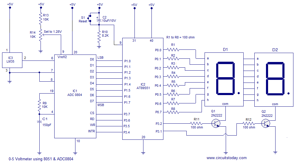
- LM35 Temperature Sensor -> ADC0804/0808 -> 8051 Microcontroller -> Output Device (Relay, Fan, Heater)
Data Flow
- The LM35 sensor produces an analog voltage corresponding to the current temperature.
- The ADC0804/0808 converts this analog voltage into a digital value.
- The 8051 microcontroller reads this digital value.
- The 8051 compares the actual temperature with the setpoint (desired temperature).
- The 8051 generates appropriate control signals based on the comparison result.
- These control signals drive the output device to increase or decrease the temperature accordingly.
Additional Considerations
- Hysteresis: Implement a small hysteresis band to prevent rapid on/off switching around the setpoint, reducing output device wear and tear.
- Display: Incorporate an LCD or LED display to visualize the current temperature.
- User Input: Add buttons or a potentiometer to adjust the desired setpoint.
Example Scenario
Let's say you want to maintain a room's temperature around 25 °C:
- The 8051 continuously reads the temperature value from the ADC.
- If the temperature falls below 24 °C, the 8051 activates a heater.
- If the temperature rises above 26 °C, the 8051 activates a fan.
GSM based Security System
Components:
-
Microcontroller (8051):
- The central processing unit (CPU) of the system.
- Reads sensor data, controls the system's logic, and communicates with other components.
-
GSM Modem:
- Enables communication with the GSM network (mobile cellular network).
- Used for sending SMS alerts or making emergency calls.
-
Sensors:
- Detect security breaches or environmental changes (e.g., door/window contacts, PIR sensors, smoke detectors, gas sensors).
- Provide input signals to the microcontroller.
-
Relay Driver:
- Drives relays that control external devices like alarms, lights, or door locks.
- The microcontroller sends control signals to the relay driver, which activates the relays accordingly.
-
Switches:
- Allow manual user interaction with the system (e.g., arming/disarming the alarm, controlling lights).
- Provide input signals to the microcontroller.
-
Power Supply:
- Provides power to all the components of the system.
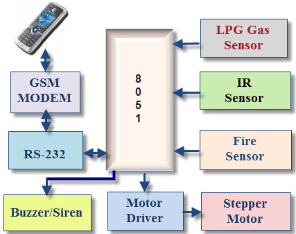
Data Flow:
- Sensors: Continuously monitor the environment for security threats.
- Microcontroller:
- Reads sensor data and processes it to detect security breaches.
- If a breach is detected, the microcontroller triggers an alarm and sends SMS alerts or makes emergency calls.
- GSM Modem:
- Communicates with the mobile network based on the microcontroller's instructions.
- Sends SMS alerts or initiates emergency calls to predefined numbers.
- Relay Driver:
- Receives control signals from the microcontroller.
- Activates or deactivates relays to control external devices like alarms, lights, or door locks.
- Switches:
- Provide user input to the microcontroller for actions like arming/disarming the system or controlling lights manually.
RPM meter
Core Components
-
Rotation Sensor:
- Generates pulses proportional to the rotational speed of the shaft you wish to measure. Several types are common:
- Inductive Pickup: Detects passing gear teeth or keyways (good for robust applications).
- Hall Effect Sensor: Detects changes in the magnetic field created by magnets attached to the rotating shaft.
- Optical Sensor: Detects light/dark patterns on a disc attached to the shaft.
- Generates pulses proportional to the rotational speed of the shaft you wish to measure. Several types are common:
-
Signal Conditioning Circuit:
- Amplification: Boosts the sensor signal to a level the microcontroller can work with (often 0-5V).
- Noise Filtering: Removes unwanted noise that could corrupt the pulse detection.
-
8051 Microcontroller:
- Pulse Counting: Counts the number of pulses from the sensor in a fixed time interval.
- RPM Calculation: Converts the pulse count over a known time interval into the revolutions per minute (RPM) value.
- Optional Output: Can drive a display or transmit RPM data over a communication bus.
-
Display (Optional)
- Presents the calculated RPM to the user. Common options:
- LCD: Alphanumeric display for showing numerical RPM values.
- LED Bar Graph: A visual representation of increasing speed.
- Presents the calculated RPM to the user. Common options:
Block Diagram
Data Flow
- Sensor: Generates electrical pulses corresponding to each rotation of the shaft.
- Signal Conditioning: Cleans and amplifies the sensor signal for the microcontroller.
- 8051:
- Measures the time between pulses or counts pulses in a fixed time interval.
- Calculates the RPM based on the pulse measurement.
- Output: Sends the calculated RPM to a display or other communication channels.
Example Calculation
If the sensor setup generates 1 pulse per rotation, and the 8051 counts 60 pulses in one second:
- RPM = 60 pulses per second * 60 seconds per minute = 3600 RPM
Enhancements
- Multiple Sensors: Use additional sensors for more accurate pulse counting to increase precision.
- Averaging: Calculate RPM over several periods and average them for a smoother reading.
- User Interface: Add buttons or a potentiometer to select different display modes or trigger calibration routines.